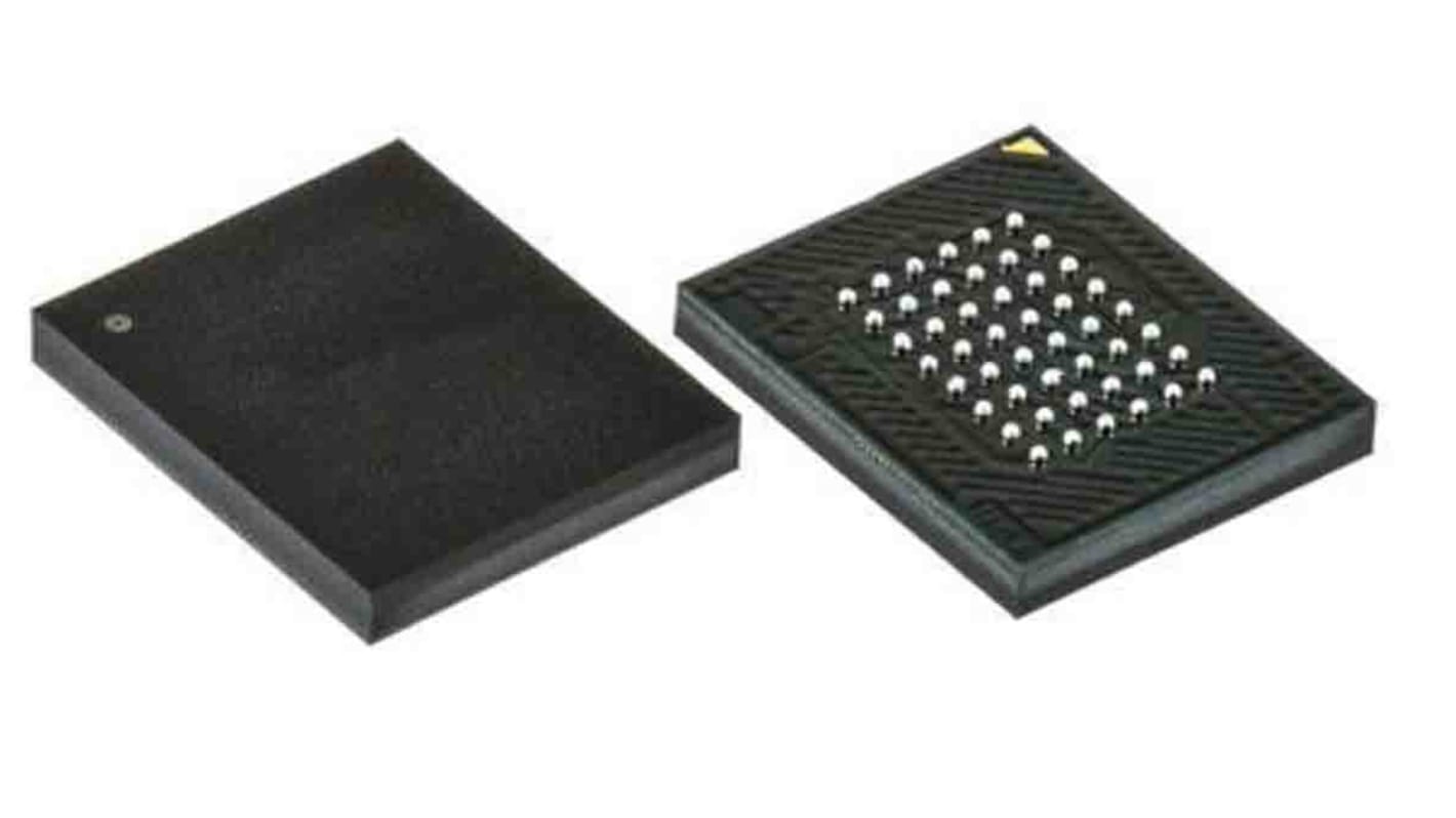
Infineon, CFI, NOR 64 MB Flash-minne, 70 ns, 48 Ben, BGA
- RS-artikelnummer:
- 193-8826
- Tillv. art.nr:
- S29GL064S70BHI030
- Tillverkare / varumärke:
- Infineon

Antal (1 förpackning med 5 enheter)*
196,76 kr
(exkl. moms)
245,95 kr
(inkl. moms)
GRATIS leverans för online beställningar över 750,00 kr
I lager
- 220 enhet(er) är redo att levereras
Behöver du mer? Ange den kvantitet du behöver och klicka på "Kontrollera leveransdatum"
Enheter | Per enhet | Per förpackning* |
|---|---|---|
| 5 + | 39,352 kr | 196,76 kr |
*vägledande pris
- RS-artikelnummer:
- 193-8826
- Tillv. art.nr:
- S29GL064S70BHI030
- Tillverkare / varumärke:
- Infineon
Specifikationer
Datablad
Lagstiftning och ursprungsland
Produktdetaljer
Hitta liknande produkter genom att välja ett eller flera attribut.
Välj alla | Attribut | Värde |
|---|---|---|
| Varumärke | Infineon | |
| Minnesstorlek | 64MB | |
| Produkttyp | Flash-minne | |
| Gränssnittstyp | CFI, | |
| Kapseltyp | BGA | |
| Antal ben | 48 | |
| Organisation | 8M x 8 bitar | |
| Typ av fäste | Yta | |
| Celltyp | NOR | |
| Maximal matningsspänning | 3.6V | |
| Minsta matningsspänning | 2.7V | |
| Tidsinställningstyp | Asynkron | |
| Minsta arbetsstemperatur | -40°C | |
| Maximal arbetstemperatur | 85°C | |
| Höjd | 0.84mm | |
| Längd | 8.15mm | |
| Standarder/godkännanden | No | |
| Bredd | 6.15mm | |
| Maximal slumpmässig åtkomsttid | 70ns | |
| Matningsström | 50mA | |
| Serie | S29GL064S | |
| Antal ord | 8K | |
| Fordonsstandard | AEC-Q100 | |
| Antal bitar per ord | 8 | |
| Välj alla | ||
|---|---|---|
Varumärke Infineon | ||
Minnesstorlek 64MB | ||
Produkttyp Flash-minne | ||
Gränssnittstyp CFI, | ||
Kapseltyp BGA | ||
Antal ben 48 | ||
Organisation 8M x 8 bitar | ||
Typ av fäste Yta | ||
Celltyp NOR | ||
Maximal matningsspänning 3.6V | ||
Minsta matningsspänning 2.7V | ||
Tidsinställningstyp Asynkron | ||
Minsta arbetsstemperatur -40°C | ||
Maximal arbetstemperatur 85°C | ||
Höjd 0.84mm | ||
Längd 8.15mm | ||
Standarder/godkännanden No | ||
Bredd 6.15mm | ||
Maximal slumpmässig åtkomsttid 70ns | ||
Matningsström 50mA | ||
Serie S29GL064S | ||
Antal ord 8K | ||
Fordonsstandard AEC-Q100 | ||
Antal bitar per ord 8 | ||
S29GL-S enhetsfamiljen med medelhög densitet är 3, 0-volts flashminne med enkel strömförsörjning som tillverkas med 65 nm MirrorBit-teknik.
S29GL064S är en 64 Mb enhet organiserad som 4 194 304 ord eller 8 388 608 byte. Beroende på modellnummer har enheterna endast en 16-bitars bred databuss, eller en 16-bitars bred databuss som också kan fungera som en 8-bitars bred databuss genom att använda BYTE#-ingången.
Enheterna kan programmeras antingen i värdsystemet eller i standard EPROM-programmerare. Åtkomsttider så snabba som 70 ns finns tillgängliga. Paketerbjudanden inkluderar 48-stifts TSOP, 56-stifts TSOP, 48-bollars BGA med fin pitch och 64-bollars Fortified BGA, beroende på modellnummer. Varje enhet har separata kontroller för chip-aktivering (CE#), skrivaktivering (WE#) och utgångsaktivering (OE#). Varje enhet kräver endast en enda 3,0-volts strömförsörjning för både läs- och skrivfunktioner. Förutom en VCC-ingång stöds en högspänningsaccelererad programfunktion (ACC) genom ökad spänning på WP#/ACC- eller ACC-ingången. Denna funktion är avsedd att underlätta systemproduktion. Kommandon skrivs till enheten med standardmikroprocessor-skrivtid. Skrivcykler kräver även interna låsadresser och data för programmerings- och raderingsoperationer.
Sektorraderarkitekturen gör det möjligt att radera och omprogrammera minnessektorer utan att påverka datainnehållet i andra sektorer. Enheten är helt raderad när den levereras från fabriken.
Det avancerade sektorskyddet har flera nivåer av sektorskydd, vilket kan avaktivera både programmet och radera operationer i vissa sektorer.
Relaterade länkar
- Infineon, CFI, NOR 64 MB Flash-minne, 70 ns, 48 Ben, BGA
- Infineon, CFI, NOR 256 MB Flash-minne, 110 ns, 64 Ben, BGA
- Infineon, CFI, 512 MB Flash-minne, 110 ns, 64 Ben, BGA
- Infineon, CFI, SPI NOR 512 MB Flash-minne, 14.5 ns, 24 Ben, BGA, 4
- Infineon, CFI, NOR 16 MB Flash-minne, 70 ns, 48 Ben, TSOP
- Infineon, CFI, NOR 8 MB Flash-minne, 70 ns, 48 Ben, TSOP
- Infineon, CFI, NOR 32 MB Flash-minne, 70 ns, 48 Ben, TSOP
- Infineon, CFI, Parallell NOR 8 MB Flash-minne, 70 ns, 48 Ben, TSOP