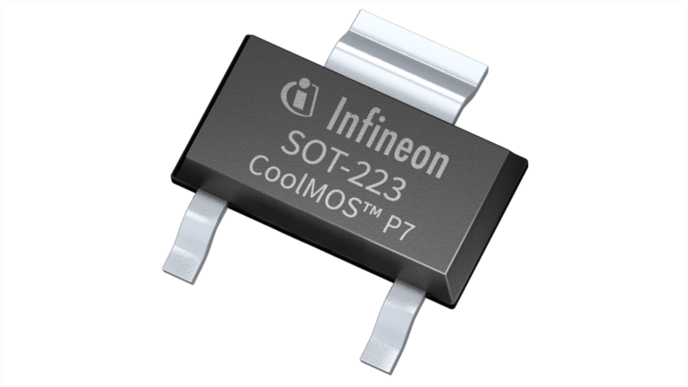
Infineon CoolMOS P7 Type N-Channel MOSFET & Diode, 16 A, 650 V Enhancement, 3-Pin SOT-223
- RS-artikelnummer:
- 220-7436
- Tillv. art.nr:
- IPN60R600P7SATMA1
- Tillverkare / varumärke:
- Infineon

Mängdrabatt möjlig
Antal (1 rulle med 3000 enheter)*
7 317,00 kr
(exkl. moms)
9 147,00 kr
(inkl. moms)
GRATIS leverans för online beställningar över 500,00 kr
Tillfälligt slut
- Leverans från den 26 oktober 2026
Behöver du mer? Ange den kvantitet du behöver och klicka på "Kontrollera leveransdatum"
Enheter | Per enhet | Per rulle* |
|---|---|---|
| 3000 - 3000 | 2,439 kr | 7 317,00 kr |
| 6000 + | 2,317 kr | 6 951,00 kr |
*vägledande pris
- RS-artikelnummer:
- 220-7436
- Tillv. art.nr:
- IPN60R600P7SATMA1
- Tillverkare / varumärke:
- Infineon
Specifikationer
Datablad
Lagstiftning och ursprungsland
Produktdetaljer
Hitta liknande produkter genom att välja ett eller flera attribut.
Välj alla | Attribut | Värde |
|---|---|---|
| Brand | Infineon | |
| Product Type | MOSFET & Diode | |
| Channel Type | Type N | |
| Maximum Continuous Drain Current Id | 16A | |
| Maximum Drain Source Voltage Vds | 650V | |
| Series | CoolMOS P7 | |
| Package Type | SOT-223 | |
| Mount Type | Surface | |
| Pin Count | 3 | |
| Maximum Drain Source Resistance Rds | 600mΩ | |
| Channel Mode | Enhancement | |
| Maximum Gate Source Voltage Vgs | 20 V | |
| Maximum Power Dissipation Pd | 7W | |
| Forward Voltage Vf | 0.9V | |
| Typical Gate Charge Qg @ Vgs | 9nC | |
| Standards/Approvals | No | |
| Width | 3.7 mm | |
| Length | 6.7mm | |
| Height | 1.8mm | |
| Automotive Standard | No | |
| Välj alla | ||
|---|---|---|
Brand Infineon | ||
Product Type MOSFET & Diode | ||
Channel Type Type N | ||
Maximum Continuous Drain Current Id 16A | ||
Maximum Drain Source Voltage Vds 650V | ||
Series CoolMOS P7 | ||
Package Type SOT-223 | ||
Mount Type Surface | ||
Pin Count 3 | ||
Maximum Drain Source Resistance Rds 600mΩ | ||
Channel Mode Enhancement | ||
Maximum Gate Source Voltage Vgs 20 V | ||
Maximum Power Dissipation Pd 7W | ||
Forward Voltage Vf 0.9V | ||
Typical Gate Charge Qg @ Vgs 9nC | ||
Standards/Approvals No | ||
Width 3.7 mm | ||
Length 6.7mm | ||
Height 1.8mm | ||
Automotive Standard No | ||
The Infineon Cool MOS P7 super junction (SJ) MOSFET is designed to address typical challenges in the low power SMPS market, by offering excellent performance and ease-of-use, enabling improved form factors and price competitiveness. The SOT-223 package is a cost effective one-to-one drop-in alternative to DPAK that also enables footprint reduction in some designs. It can be placed on a typical DPAK footprint and shows comparable thermal performance. This combination makes Cool MOS P7 in SOT-223 a perfect fit for its target applications. The 700V and 800V Cool MOS P7 are optimized for fly back topologies. 600V Cool MOS P7 SJ MOSFET is suitable for hard as well as so switching topologies (Fly back, PFC and LLC).
Ease of use and fast design-in through low ringing tendency and usage
across PFC and PWM stages
Simplified thermal management due to low switching and conduction
losses
Increased power density solutions enabled by using product swith
smaller foot print and higher manufacturing quality due to>2kVESD
protection
Suitable for awide variety of applications and power ranges
relaterade länkar
- Infineon CoolMOS P7 Type N-Channel MOSFET & Diode 650 V Enhancement, 3-Pin SOT-223 IPN60R600P7SATMA1
- Infineon CoolMOS P7 Type N-Channel MOSFET 800 V Enhancement, 3-Pin SOT-223
- Infineon CoolMOS P7 Type N-Channel MOSFET 950 V Enhancement, 3-Pin SOT-223
- Infineon CoolMOS P7 Type N-Channel MOSFET 800 V Enhancement, 3-Pin SOT-223
- Infineon CoolMOS P7 Type N-Channel MOSFET 800 V Enhancement, 3-Pin SOT-223
- Infineon CoolMOS P7 Type N-Channel MOSFET 800 V Enhancement, 3-Pin SOT-223
- Infineon CoolMOS P7 Type N-Channel MOSFET 800 V Enhancement, 3-Pin SOT-223 IPN80R600P7ATMA1
- Infineon CoolMOS P7 Type N-Channel MOSFET 800 V Enhancement, 3-Pin SOT-223 IPN80R900P7ATMA1