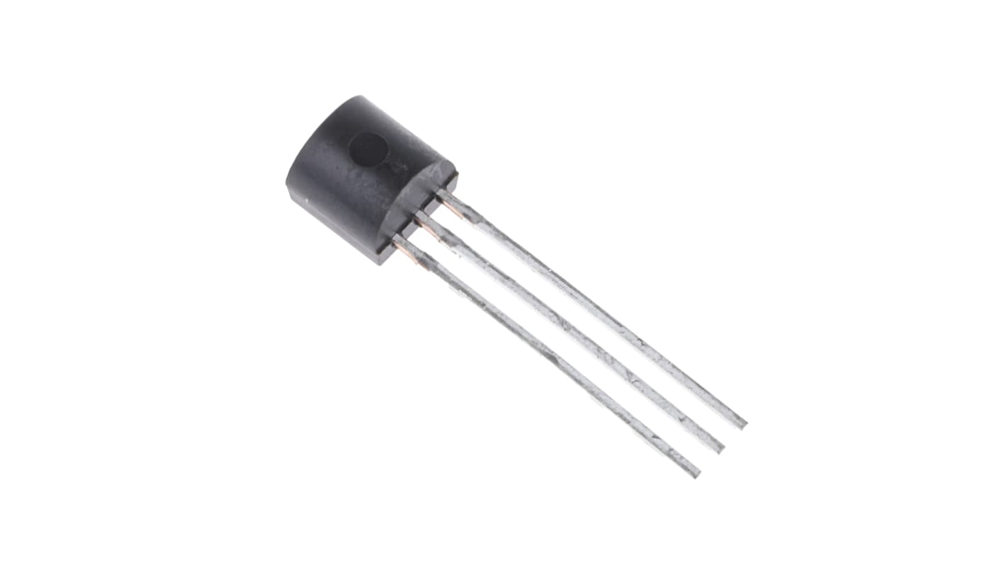
Microchip 2N7000 Type N-Channel MOSFET, 200 mA, 60 V Enhancement, 3-Pin TO-92
- RS-artikelnummer:
- 177-9588
- Tillv. art.nr:
- 2N7000-G
- Tillverkare / varumärke:
- Microchip

Antal (1 påse med 1000 enheter)*
3 629,00 kr
(exkl. moms)
4 536,00 kr
(inkl. moms)
GRATIS leverans för online beställningar över 500,00 kr
Tillfälligt slut
- 3 000 enhet(er) är redo att levereras
Behöver du mer? Ange den kvantitet du behöver och klicka på "Kontrollera leveransdatum"
Enheter | Per enhet | Per Påse* |
|---|---|---|
| 1000 + | 3,629 kr | 3 629,00 kr |
*vägledande pris
- RS-artikelnummer:
- 177-9588
- Tillv. art.nr:
- 2N7000-G
- Tillverkare / varumärke:
- Microchip
Specifikationer
Datablad
Lagstiftning och ursprungsland
Produktdetaljer
Hitta liknande produkter genom att välja ett eller flera attribut.
Välj alla | Attribut | Värde |
|---|---|---|
| Brand | Microchip | |
| Product Type | MOSFET | |
| Channel Type | Type N | |
| Maximum Continuous Drain Current Id | 200mA | |
| Maximum Drain Source Voltage Vds | 60V | |
| Package Type | TO-92 | |
| Series | 2N7000 | |
| Mount Type | Through Hole | |
| Pin Count | 3 | |
| Maximum Drain Source Resistance Rds | 5.3Ω | |
| Channel Mode | Enhancement | |
| Minimum Operating Temperature | -55°C | |
| Maximum Power Dissipation Pd | 1W | |
| Maximum Gate Source Voltage Vgs | 30 V | |
| Forward Voltage Vf | 0.85V | |
| Maximum Operating Temperature | 150°C | |
| Standards/Approvals | No | |
| Length | 5.08mm | |
| Height | 5.33mm | |
| Width | 4.06 mm | |
| Automotive Standard | No | |
| Välj alla | ||
|---|---|---|
Brand Microchip | ||
Product Type MOSFET | ||
Channel Type Type N | ||
Maximum Continuous Drain Current Id 200mA | ||
Maximum Drain Source Voltage Vds 60V | ||
Package Type TO-92 | ||
Series 2N7000 | ||
Mount Type Through Hole | ||
Pin Count 3 | ||
Maximum Drain Source Resistance Rds 5.3Ω | ||
Channel Mode Enhancement | ||
Minimum Operating Temperature -55°C | ||
Maximum Power Dissipation Pd 1W | ||
Maximum Gate Source Voltage Vgs 30 V | ||
Forward Voltage Vf 0.85V | ||
Maximum Operating Temperature 150°C | ||
Standards/Approvals No | ||
Length 5.08mm | ||
Height 5.33mm | ||
Width 4.06 mm | ||
Automotive Standard No | ||
- COO (Country of Origin):
- TW
Microchip Technology MOSFET
The Microchip Technology through-hole mount N-channel MOSFET is a new age product with a drain-source voltage of 60V and a maximum gate-source voltage of 30V. It has drain-source resistance of 5ohms at a gate-source voltage of 10V. It has continuous drain current of 200mA and maximum power dissipation of 1W. The minimum and a maximum driving voltage for this MOSFET is 4.5V and 10V respectively. The MOSFET is an enhancement mode (normally off) MOSFET that utilizes a vertical DMOS structure and well-proven, silicon gate manufacturing process. This combination produces a device with the power handling capabilities of bipolar transistors and the high input impedance and positive temperature coefficient inherent in MOS devices. A significant characteristic of all MOS structures, this device is free from thermal runaway and thermally induced secondary breakdown. This vertical DMOS FET has been optimized for lower switching and conduction losses. The MOSFET offers excellent efficiency along with a long and productive life without compromising performance or functionality.
Features and Benefits
• Ease of paralleling
• Excellent thermal stability
• Free from secondary breakdown
• High input impedance and high gain
• Integral source drain diode
• Low CISS and fast switching speeds
• Low power drive requirement
• Operating temperature ranges between -55°C and 150°C
Applications
• Amplifiers
• Converters
• Drivers: relays, hammers, solenoids, lamps, memories, displays, bipolar transistors, etc.
• Motor controls
• Power supply circuits
• Switches
Certifications
• ANSI/ESD S20.20:2014
• BS EN 61340-5-1:2007
• JEDEC
relaterade länkar
- Microchip 2N7000 Type N-Channel MOSFET 60 V Enhancement, 3-Pin TO-92 2N7000-G
- onsemi 2N7000 Type N-Channel MOSFET 60 V Enhancement, 3-Pin TO-92 2N7000
- onsemi 2N7000 Type N-Channel MOSFET 60 V Enhancement, 3-Pin TO-92 2N7000-D26Z
- onsemi 2N7000 Type N-Channel MOSFET 60 V Enhancement, 3-Pin TO-92
- onsemi 2N7000 Type N-Channel MOSFET 60 V Enhancement, 3-Pin TO-92 2N7000TA
- Microchip Type N-Channel MOSFET 60 V Enhancement, 3-Pin TO-92
- Microchip VN10K Type N-Channel MOSFET 60 V Enhancement, 3-Pin TO-92
- Microchip 2N7008 Type N-Channel MOSFET 60 V Enhancement, 3-Pin TO-92