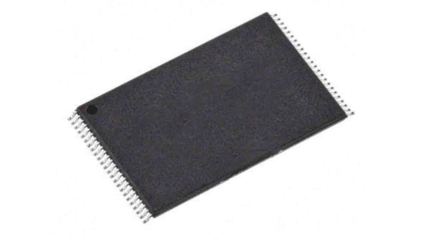
Infineon, CFI, NOR 8 MB Flash-minne, 70 ns, 48 Ben, TSOP
- RS-artikelnummer:
- 193-8784
- Tillv. art.nr:
- S29AL008J70TFI013
- Tillverkare / varumärke:
- Infineon

För närvarande inte tillgänglig
Vi vet inte om den här artikeln kommer tillbaka i lager, RS har för avsikt att ta bort den från vårt utbud snart.
- RS-artikelnummer:
- 193-8784
- Tillv. art.nr:
- S29AL008J70TFI013
- Tillverkare / varumärke:
- Infineon
Specifikationer
Datablad
Lagstiftning och ursprungsland
Produktdetaljer
Hitta liknande produkter genom att välja ett eller flera attribut.
Välj alla | Attribut | Värde |
|---|---|---|
| Varumärke | Infineon | |
| Minnesstorlek | 8MB | |
| Produkttyp | Flash-minne | |
| Gränssnittstyp | CFI, | |
| Kapseltyp | TSOP | |
| Antal ben | 48 | |
| Typ av fäste | Yta | |
| Celltyp | NOR | |
| Maximal matningsspänning | 3.6V | |
| Minsta matningsspänning | 2.7V | |
| Tidsinställningstyp | Asynkron | |
| Minsta arbetsstemperatur | -40°C | |
| Maximal arbetstemperatur | 85°C | |
| Standarder/godkännanden | No | |
| Höjd | 1.05mm | |
| Längd | 12mm | |
| Maximal slumpmässig åtkomsttid | 70ns | |
| Antal bitar per ord | 8 | |
| Matningsström | 20mA | |
| Serie | S29AL008J | |
| Fordonsstandard | AEC-Q100 | |
| Antal ord | 1M | |
| Välj alla | ||
|---|---|---|
Varumärke Infineon | ||
Minnesstorlek 8MB | ||
Produkttyp Flash-minne | ||
Gränssnittstyp CFI, | ||
Kapseltyp TSOP | ||
Antal ben 48 | ||
Typ av fäste Yta | ||
Celltyp NOR | ||
Maximal matningsspänning 3.6V | ||
Minsta matningsspänning 2.7V | ||
Tidsinställningstyp Asynkron | ||
Minsta arbetsstemperatur -40°C | ||
Maximal arbetstemperatur 85°C | ||
Standarder/godkännanden No | ||
Höjd 1.05mm | ||
Längd 12mm | ||
Maximal slumpmässig åtkomsttid 70ns | ||
Antal bitar per ord 8 | ||
Matningsström 20mA | ||
Serie S29AL008J | ||
Fordonsstandard AEC-Q100 | ||
Antal ord 1M | ||
The S29AL008J is a 8 Mbit, 3.0 Volt-only Flash memory organized as 1,048,576 bytes or 524,288 words. The device is offered in 48-ball Fine-pitch BGA (0.8 mm pitch) and 48pin TSOP packages. The word-wide data (x16) appears on DQ15–DQ0, the byte-wide (x8) data appears on DQ7–DQ0. This device is designed to be programmed in-system with the standard system 3.0 volt VCC supply. A 12.0 V VPP or 5.0 VCC are not required for write or erase operations. The device can also be programmed in standard EPROM programmers.
The device offers access times of up to 55 ns allowing high speed microprocessors to operate without wait states. To eliminate bus contention the device has separate chip enable (CE#), write enable (WE#) and output enable (OE#) controls.
Device programming occurs by executing the program command sequence. This initiates the Embedded Program algorithm an internal algorithm that automatically times the program pulse widths and verifies proper cell margin. The Unlock Bypass mode facilitates faster programming times by requiring only two write cycles to program data instead of four.
Device erasure occurs by executing the erase command sequence. This initiates the Embedded Erase algorithm an internal algorithm that automatically preprograms the array (if it is not already programmed) before executing the erase operation. Duringerase, the device automatically times the erase pulse widths and verifies proper cell margin. The host system can detect whether a program or erase operation is complete by observing the RY/BY# pin, or by reading the DQ7(Data# Polling) and DQ6 (toggle) status bits. After a program or erase cycle has been completed, the device is ready to read array data or accept another command.
Relaterade länkar
- Infineon NOR 8 MB Flash-minne 48 Ben, TSOP
- Infineon NOR 16 MB Flash-minne 48 Ben, TSOP
- Infineon NOR 32 MB Flash-minne 48 Ben, TSOP
- Infineon Parallell NOR 8 MB Flash-minne 48 Ben, TSOP
- Infineon NOR 1024 MB Flash-minne 56 Ben, TSOP
- Infineon Parallell NOR 512 MB Flash-minne 56 Ben, TSOP
- Infineon CFI 90 ns TSOP
- Infineon Parallell NOR 128 MB Flash-minne 56 Ben, TSOP