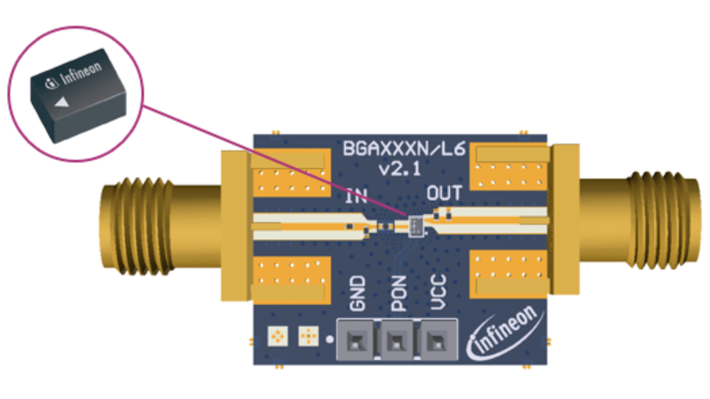
Infineon Ultra Low Current Low Noise Amplifier for L2/L5 GNSS Applications Diode Low Noise Amplifier Evaluation Board
- RS-artikelnummer:
- 273-2072
- Tillv. art.nr:
- EVALBGA125N6TOBO1
- Tillverkare / varumärke:
- Infineon

Mängdrabatt möjlig
Antal (1 enhet)*
2 213,68 kr
(exkl. moms)
2 767,10 kr
(inkl. moms)
GRATIS leverans för online beställningar över 500,00 kr
I lager
- 4 enhet(er) är redo att levereras
Behöver du mer? Ange den kvantitet du behöver och klicka på "Kontrollera leveransdatum"
Enheter | Per enhet |
|---|---|
| 1 - 4 | 2 213,68 kr |
| 5 - 9 | 2 103,14 kr |
| 10 + | 2 047,70 kr |
*vägledande pris
- RS-artikelnummer:
- 273-2072
- Tillv. art.nr:
- EVALBGA125N6TOBO1
- Tillverkare / varumärke:
- Infineon
Specifikationer
Datablad
Lagstiftning och ursprungsland
Produktdetaljer
Hitta liknande produkter genom att välja ett eller flera attribut.
Välj alla | Attribut | Värde |
|---|---|---|
| Brand | Infineon | |
| Classification | GNSS Module | |
| RF Technology | Low Noise Amplifier | |
| Technology | Amplifier & Linear | |
| Kit Classification | Evaluation Board | |
| For Use With | Mobile Cellular | |
| Featured Device | Diode | |
| Frequency | 1300MHz | |
| Kit Name | Ultra Low Current Low Noise Amplifier for L2/L5 GNSS Applications | |
| Välj alla | ||
|---|---|---|
Brand Infineon | ||
Classification GNSS Module | ||
RF Technology Low Noise Amplifier | ||
Technology Amplifier & Linear | ||
Kit Classification Evaluation Board | ||
For Use With Mobile Cellular | ||
Featured Device Diode | ||
Frequency 1300MHz | ||
Kit Name Ultra Low Current Low Noise Amplifier for L2/L5 GNSS Applications | ||
- COO (Country of Origin):
- DE
Infineon Communication & Wireless Development Tool, Low Noise Amplifier RF Technology, GNSS Module Classification - EVALBGA125N6TOBO1
This communication and wireless development tool is an ultra low current low noise amplifier designed specifically for L2/L5 GNSS applications. It operates within the frequency range of 1164 to 1300 MHz and features dimensions of 0.7 x 1.1 mm². The device is particularly beneficial for mobile cellular IoT solutions, ensuring exceptional performance while minimising power consumption.
Features & Benefits
• Ultra low power consumption of just 1.3mA enhances battery life
• High insertion power gain of 20dB optimises signal strength
• Low noise figure of 0.80dB ensures improved sensitivity
• Compact, RoHS/WEEE compliant package supports diverse requirements
• High insertion power gain of 20dB optimises signal strength
• Low noise figure of 0.80dB ensures improved sensitivity
• Compact, RoHS/WEEE compliant package supports diverse requirements
Applications
• Ideal for enhancing GNSS signal sensitivity in wearables
• Suitable for integration into mobile cellular technology
• Utilised in high-frequency requiring low noise solutions
• Designed for evaluation boards targeting GNSS application development
• Supports application development leveraging RF technology solutions
• Suitable for integration into mobile cellular technology
• Utilised in high-frequency requiring low noise solutions
• Designed for evaluation boards targeting GNSS application development
• Supports application development leveraging RF technology solutions
What benefits does operating at a frequency range of 1164 to 1300 MHz provide for my project?
Utilising this frequency range enhances GNSS signal sensitivity, ensuring reliable positioning and navigation, which is especially critical for mobile and wearable devices.
How does the low power consumption of 1.3 mA impact device performance?
The ultra low current consumption significantly extends battery life in portable devices, making it ideal for applications where power efficiency is paramount.
What advantages does the wide supply voltage range offer for design?
The flexibility of a supply voltage range from 1.1V to 2.8V supports various system designs and increases compatibility with different power sources, accommodating diverse applications.
How does the low noise figure improve the device's effectiveness in GNSS applications?
A low noise figure reduces background noise, enhancing signal clarity and allowing for better detection of weak signals in challenging environments, ensuring reliable performance.
What ESD protection mechanisms are integrated to ensure the device's durability?
The built-in 2kV HBM ESD protection assists in safeguarding the device from electrostatic discharge risks, thereby enhancing its reliability in various operational environments.
relaterade länkar
- Infineon Ultra Low Current Low Noise Amplifier for GNSS Applications Diode Low Noise Amplifier Evaluation Board for
- Infineon Small Footprint Ultra Low Current Low Noise Amplifier for Global Navigation Sattelite System Diode Low Noise
- BGA7H1N6E6327XTSA1 Infineon 12.5 dB 2690 MHz, 6-Pin TSNP-6-2
- BGA7L1BN6E6327XTSA1 Infineon 13.6 dB 960 MHz, 6-Pin TSNP-6-2
- BGB707L7ESDE6327XTSA1 Infineon 31.5 dB 5.6 GHz TSLP-7-1
- BGA715N7E6327XTSA2 Infineon 20 dB 1.615 GHz, 7-Pin TSNP
- BGA524N6E6327XTSA1 Infineon 19.6 dB 1615 MHz, 6-Pin TSNP-6
- Keysight Technologies W9069EM0E Noise Figure Measurement Application