85104AGILF, Clock Buffer, 5-Input, 20-Pin TSSOP
- RS-artikelnummer:
- 216-6210P
- Tillv. art.nr:
- 85104AGILF
- Tillverkare / varumärke:
- Renesas Electronics

Mängdrabatt möjlig
Antal 10 enheter (levereras i ett rör)*
1 369,80 kr
(exkl. moms)
1 712,20 kr
(inkl. moms)
GRATIS leverans för online beställningar över 500,00 kr
Sista RS lager
- Slutlig(a) 222 enhet(er), redo att levereras
Enheter | Per enhet |
|---|---|
| 10 - 24 | 136,98 kr |
| 25 - 49 | 133,39 kr |
| 50 - 99 | 129,92 kr |
| 100 + | 126,67 kr |
*vägledande pris
- RS-artikelnummer:
- 216-6210P
- Tillv. art.nr:
- 85104AGILF
- Tillverkare / varumärke:
- Renesas Electronics
Specifikationer
Datablad
Lagstiftning och ursprungsland
Produktdetaljer
Hitta liknande produkter genom att välja ett eller flera attribut.
Välj alla | Attribut | Värde |
|---|---|---|
| Brand | Renesas Electronics | |
| Logic Function | Clock Buffer | |
| Number of Clock Inputs | 5 | |
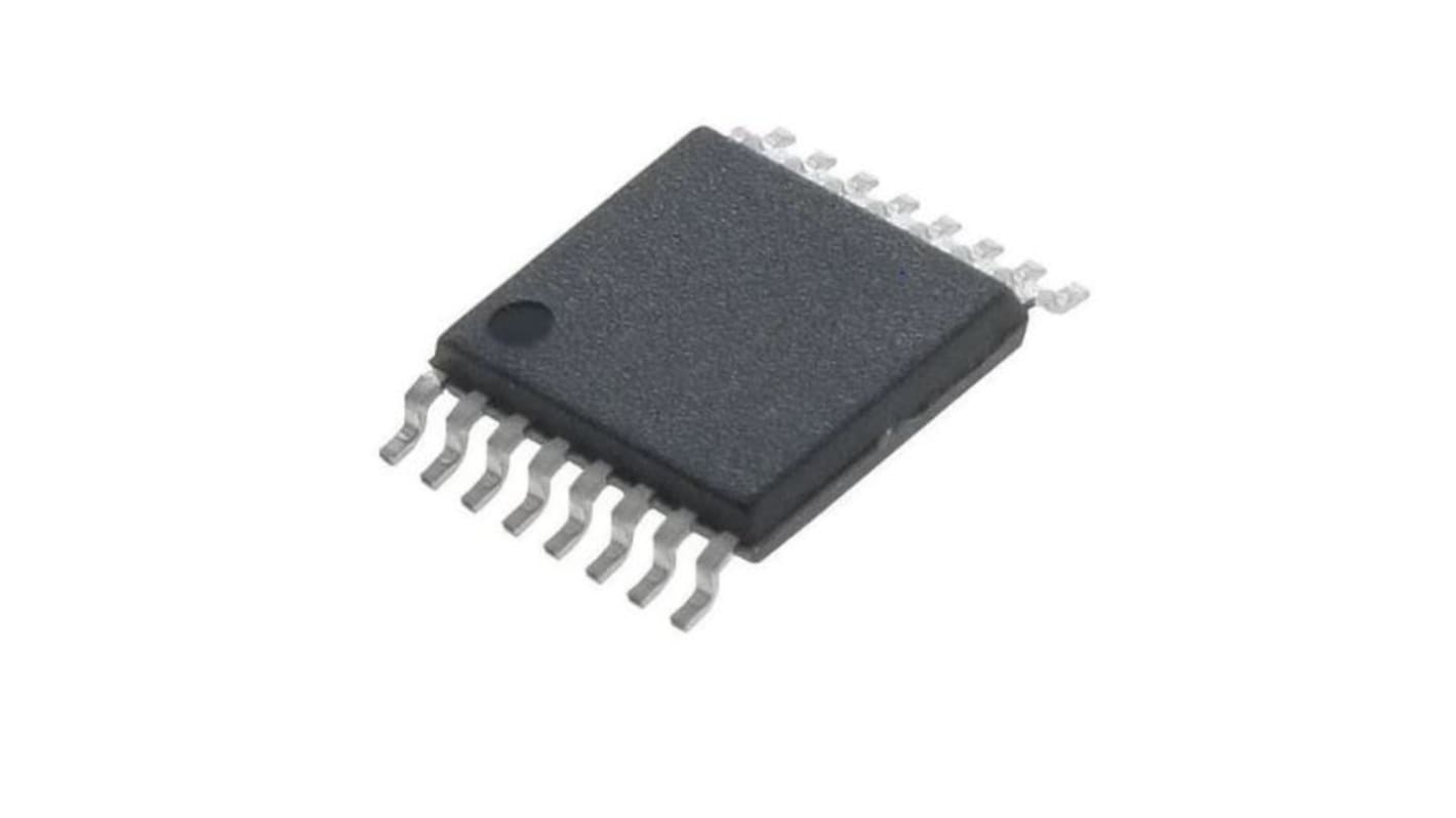
| Package Type | TSSOP | |
| Pin Count | 20 | |
| Välj alla | ||
|---|---|---|
Brand Renesas Electronics | ||
Logic Function Clock Buffer | ||
Number of Clock Inputs 5 | ||
Package Type TSSOP | ||
Pin Count 20 | ||
The Renesas Electronics 85104I is a low skew, high performance 1-to-4 Differential/LVCMOS-to-0.7V HCSL Fanout Buffer. The 85104I has two selectable clock inputs. The CLK0, nCLK0 pair can accept most standard differential input levels. The single-ended CLK1 can accept LVCMOS or LVTTL input levels. The clock enable is internally synchronized to eliminate runt clock pulses on the outputs during asynchronous assertion/deassertion of the clock enable pin.
Four 0.7V differential HCSL outputs
Selectable differential CLK0, nCLK0 or LVCMOS inputs
CLK0, nCLK0 pair can accept the following differential
input levels: LVPECL, LVDS, LVHSTL, HCSL
CLK1 can accept the following input levels:
LVCMOS or LVTTL
Maximum output frequency: 500MHz
Translates any single-ended input signal to 3.3V
HCSL levels with resistor bias on nCLK input
Output skew: 100ps (maximum)
Part-to-part skew: 600ps (maximum)
Propagation delay: 3.2ns (maximum)
Additive phase jitter, RMS: 0.22ps (typical)