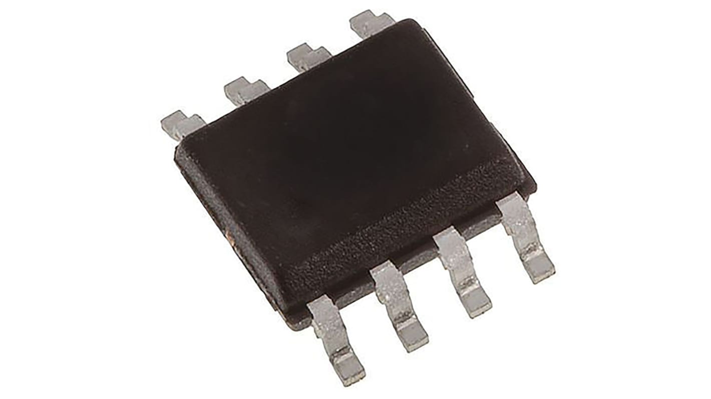
Infineon Isolated HEXFET 2 Type P, Type N-Channel MOSFET, 3.5 A, 30 V Enhancement, 8-Pin SOIC IRF9952TRPBF
- RS-artikelnummer:
- 827-3934
- Tillv. art.nr:
- IRF9952TRPBF
- Tillverkare / varumärke:
- Infineon

Mängdrabatt möjlig
Antal (1 förpackning med 20 enheter)*
132,94 kr
(exkl. moms)
166,18 kr
(inkl. moms)
GRATIS leverans för online beställningar över 500,00 kr
I lager
- Dessutom levereras 340 enhet(er) från den 19 januari 2026
- Dessutom levereras 3 640 enhet(er) från den 26 januari 2026
Behöver du mer? Ange den kvantitet du behöver och klicka på "Kontrollera leveransdatum"
Enheter | Per enhet | Per förpackning* |
|---|---|---|
| 20 - 80 | 6,647 kr | 132,94 kr |
| 100 - 180 | 5,119 kr | 102,38 kr |
| 200 - 480 | 4,788 kr | 95,76 kr |
| 500 - 980 | 4,452 kr | 89,04 kr |
| 1000 + | 4,122 kr | 82,44 kr |
*vägledande pris
- RS-artikelnummer:
- 827-3934
- Tillv. art.nr:
- IRF9952TRPBF
- Tillverkare / varumärke:
- Infineon
Specifikationer
Datablad
Lagstiftning och ursprungsland
Produktdetaljer
Hitta liknande produkter genom att välja ett eller flera attribut.
Välj alla | Attribut | Värde |
|---|---|---|
| Brand | Infineon | |
| Channel Type | Type P, Type N | |
| Product Type | MOSFET | |
| Maximum Continuous Drain Current Id | 3.5A | |
| Maximum Drain Source Voltage Vds | 30V | |
| Package Type | SOIC | |
| Series | HEXFET | |
| Mount Type | Surface | |
| Pin Count | 8 | |
| Maximum Drain Source Resistance Rds | 400mΩ | |
| Channel Mode | Enhancement | |
| Minimum Operating Temperature | -55°C | |
| Forward Voltage Vf | 0.82V | |
| Maximum Power Dissipation Pd | 2W | |
| Maximum Gate Source Voltage Vgs | 20 V | |
| Typical Gate Charge Qg @ Vgs | 6.1nC | |
| Maximum Operating Temperature | 150°C | |
| Transistor Configuration | Isolated | |
| Standards/Approvals | No | |
| Width | 4 mm | |
| Length | 5mm | |
| Height | 1.5mm | |
| Number of Elements per Chip | 2 | |
| Automotive Standard | No | |
| Välj alla | ||
|---|---|---|
Brand Infineon | ||
Channel Type Type P, Type N | ||
Product Type MOSFET | ||
Maximum Continuous Drain Current Id 3.5A | ||
Maximum Drain Source Voltage Vds 30V | ||
Package Type SOIC | ||
Series HEXFET | ||
Mount Type Surface | ||
Pin Count 8 | ||
Maximum Drain Source Resistance Rds 400mΩ | ||
Channel Mode Enhancement | ||
Minimum Operating Temperature -55°C | ||
Forward Voltage Vf 0.82V | ||
Maximum Power Dissipation Pd 2W | ||
Maximum Gate Source Voltage Vgs 20 V | ||
Typical Gate Charge Qg @ Vgs 6.1nC | ||
Maximum Operating Temperature 150°C | ||
Transistor Configuration Isolated | ||
Standards/Approvals No | ||
Width 4 mm | ||
Length 5mm | ||
Height 1.5mm | ||
Number of Elements per Chip 2 | ||
Automotive Standard No | ||
Infineon HEXFET Series MOSFET, 2.3A/3.5A Maximum Continuous Drain Current, 2W Maximum Power Dissipation - IRF9952TRPBF
This versatile MOSFET delivers high performance in a Compact package, integrating both N-channel and P-channel configurations. It is designed for effective operation in various electronic applications, ensuring efficiency and dependability. With a maximum drain current of 3.5A and a maximum drain-source voltage of 30V, it is suitable for applications that require robust switching capabilities.
Features & Benefits
• Dual-channel configuration enhances design flexibility
• Surface mount design simplifies PCB assembly
• Low resistance (150mΩ and 400mΩ) reduces power loss
• High temperature operation (+150°C) ensures reliability in extreme conditions
• Improved gate charge characteristics enhance switching efficiency
• Isolated transistor configuration minimises cross-talk for cleaner signals
Applications
• Power management solutions
• Electric vehicle systems for improved efficiency
• Industrial automation and control
• Renewable energy systems for optimal performance
• Consumer electronics for enhanced device performance
How does the isolation of this device benefit my application?
The isolated configuration minimises interference among circuits, ensuring clean signals and preventing unwanted interactions between components.
What temperature range can this device handle during operation?
It can operate within a temperature range of -55°C to +150°C, making it suitable for extreme conditions.
Can I use this product in my surface mount PCB design?
Yes, its surface mount design allows for easy integration into PCB layouts, optimising space and enhancing thermal performance.
What factors should I consider when using this for switching applications?
Ensure the maximum gate-source voltage of ±20V is not exceeded and verify that the gate charge aligns with your switching frequency for optimal performance.
How do the specifications affect my power efficiency?
With low on-resistance and high continuous drain current, this MOSFET contributes to minimal power loss, enhancing overall energy efficiency in your circuit designs.
relaterade länkar
- Infineon Isolated HEXFET 2 Type P 3.5 A 8-Pin SOIC
- Infineon Isolated HEXFET 2 Type P 3.5 A 8-Pin SOIC
- Infineon Isolated HEXFET 2 Type P 3.5 A 8-Pin SOIC IRF7105TRPBF
- Infineon Isolated HEXFET 2 Type N 4 A 8-Pin SOIC
- Infineon Isolated HEXFET 2 Type P 7.3 A 8-Pin SOIC
- Infineon Isolated HEXFET 2 Type P 6.5 A 8-Pin SOIC
- Infineon Isolated HEXFET 2 Type P-Channel MOSFET 30 V Enhancement, 8-Pin SOIC
- Infineon Isolated HEXFET 2 Type P-Channel MOSFET 20 V Enhancement, 8-Pin SOIC