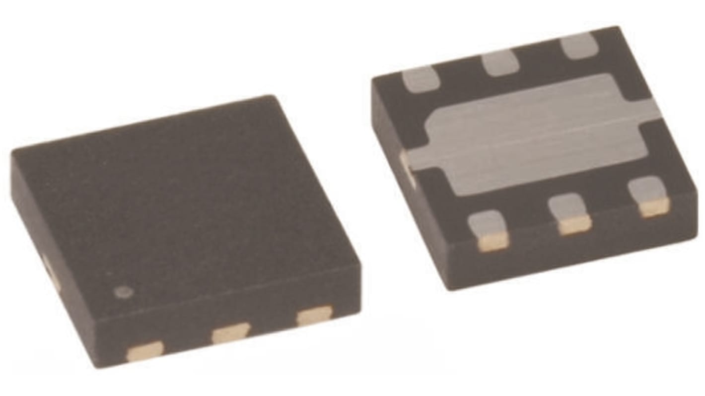
onsemi PowerTrench Type P-Channel MOSFET, 10 A, 12 V Enhancement, 6-Pin MLP
- RS-artikelnummer:
- 166-3187
- Tillv. art.nr:
- FDMA905P
- Tillverkare / varumärke:
- onsemi

För närvarande inte tillgänglig
Vi vet inte om den här artikeln kommer tillbaka i lager, RS har för avsikt att ta bort den från vårt utbud snart.
- RS-artikelnummer:
- 166-3187
- Tillv. art.nr:
- FDMA905P
- Tillverkare / varumärke:
- onsemi
Specifikationer
Datablad
Lagstiftning och ursprungsland
Produktdetaljer
Hitta liknande produkter genom att välja ett eller flera attribut.
Välj alla | Attribut | Värde |
|---|---|---|
| Brand | onsemi | |
| Product Type | MOSFET | |
| Channel Type | Type P | |
| Maximum Continuous Drain Current Id | 10A | |
| Maximum Drain Source Voltage Vds | 12V | |
| Series | PowerTrench | |
| Package Type | MLP | |
| Mount Type | Surface | |
| Pin Count | 6 | |
| Maximum Drain Source Resistance Rds | 82mΩ | |
| Channel Mode | Enhancement | |
| Maximum Power Dissipation Pd | 2.4W | |
| Maximum Gate Source Voltage Vgs | 8 V | |
| Forward Voltage Vf | -1.2V | |
| Typical Gate Charge Qg @ Vgs | 21nC | |
| Minimum Operating Temperature | -55°C | |
| Maximum Operating Temperature | 150°C | |
| Length | 2mm | |
| Standards/Approvals | No | |
| Width | 2 mm | |
| Height | 0.725mm | |
| Automotive Standard | No | |
| Välj alla | ||
|---|---|---|
Brand onsemi | ||
Product Type MOSFET | ||
Channel Type Type P | ||
Maximum Continuous Drain Current Id 10A | ||
Maximum Drain Source Voltage Vds 12V | ||
Series PowerTrench | ||
Package Type MLP | ||
Mount Type Surface | ||
Pin Count 6 | ||
Maximum Drain Source Resistance Rds 82mΩ | ||
Channel Mode Enhancement | ||
Maximum Power Dissipation Pd 2.4W | ||
Maximum Gate Source Voltage Vgs 8 V | ||
Forward Voltage Vf -1.2V | ||
Typical Gate Charge Qg @ Vgs 21nC | ||
Minimum Operating Temperature -55°C | ||
Maximum Operating Temperature 150°C | ||
Length 2mm | ||
Standards/Approvals No | ||
Width 2 mm | ||
Height 0.725mm | ||
Automotive Standard No | ||
PowerTrench® P-Channel MOSFET, Fairchild Semiconductor
PowerTrench® MOSFETs are optimised power switches that offer increase of system efficiency and power density. They combine small gate charge(Qg), small reverse recovery charge(Qrr) and soft reverse recovery body diode, which contributes to fast switching of synchronous rectification in AC/DC power supplies.
The latest PowerTrench® MOSFETs employa shielded-gate structure that provides charge balance. By utilizing this Advanced technology, the FOM (Figure of Merit) of these devices is significant lower than that of previous generations.
Soft body diode performance of the PowerTrench® MOSFETs is able to eliminate snubber circuits or replace a higher voltage rating MOSFET.
MOSFET Transistors, ON Semi
ON Semi offers a substantial portfolio of MOSFET devices that includes high-voltage (>250V) and low-voltage (<250V) types. The Advanced silicon technology provides smaller die sizes, which it is incorporated into multiple industry-standard and thermally-enhanced packages.
ON Semi MOSFETs provide superior design reliability from reduced voltage spikes and overshoot, to lower junction capacitance and reverse recovery charge, to elimination of additional external components to keep systems up and running longer.
relaterade länkar
- onsemi PowerTrench Type P-Channel MOSFET 12 V Enhancement, 6-Pin MLP FDMA905P
- onsemi PowerTrench Type P-Channel MOSFET 12 V Enhancement, 6-Pin MLP
- onsemi PowerTrench Type P-Channel MOSFET 12 V Enhancement, 6-Pin MLP FDME905PT
- onsemi PowerTrench Type P-Channel MOSFET 20 V Enhancement, 6-Pin MLP
- onsemi PowerTrench Type P-Channel MOSFET 20 V Enhancement, 6-Pin MLP FDMA910PZ
- onsemi Isolated PowerTrench 2 Type P-Channel MOSFET 30 V Enhancement, 6-Pin MLP
- onsemi Isolated PowerTrench 2 Type P-Channel MOSFET 20 V Enhancement, 6-Pin MLP
- onsemi Isolated PowerTrench 2 Type P-Channel MOSFET 20 V Enhancement, 6-Pin MLP FDMA1023PZ