Digilent 410-300 GENESYS2 KINTEX-7 Development Board ADC1410 for DAC121S101
- RS-artikelnummer:
- 134-6471
- Distrelec artikelnummer:
- 300-44-262
- Tillv. art.nr:
- 410-300
- Tillverkare / varumärke:
- Digilent

Mängdrabatt möjlig
Antal (1 enhet)*
11 762,34 kr
(exkl. moms)
14 702,92 kr
(inkl. moms)
GRATIS leverans för online beställningar över 500,00 kr
Tillfälligt slut
- 8 enhet(er) levereras från den 30 januari 2026
- Dessutom levereras 34 enhet(er) från den 06 februari 2026
Behöver du mer? Ange den kvantitet du behöver och klicka på "Kontrollera leveransdatum"
Enheter | Per enhet |
|---|---|
| 1 - 1 | 11 762,34 kr |
| 2 - 4 | 11 291,73 kr |
| 5 + | 10 350,82 kr |
*vägledande pris
- RS-artikelnummer:
- 134-6471
- Distrelec artikelnummer:
- 300-44-262
- Tillv. art.nr:
- 410-300
- Tillverkare / varumärke:
- Digilent
Specifikationer
Datablad
Lagstiftning och ursprungsland
Produktdetaljer
Hitta liknande produkter genom att välja ett eller flera attribut.
Välj alla | Attribut | Värde |
|---|---|---|
| Brand | Digilent | |
| Product Type | Plug-In Module | |
| Kit Classification | Development Board | |
| Programmable Logic Technology | FPGA | |
| For Use With | DAC121S101 | |
| Featured Device | ADC1410 | |
| Kit Name | GENESYS2 KINTEX-7 | |
| Standards/Approvals | RoHS | |
| Välj alla | ||
|---|---|---|
Brand Digilent | ||
Product Type Plug-In Module | ||
Kit Classification Development Board | ||
Programmable Logic Technology FPGA | ||
For Use With DAC121S101 | ||
Featured Device ADC1410 | ||
Kit Name GENESYS2 KINTEX-7 | ||
Standards/Approvals RoHS | ||
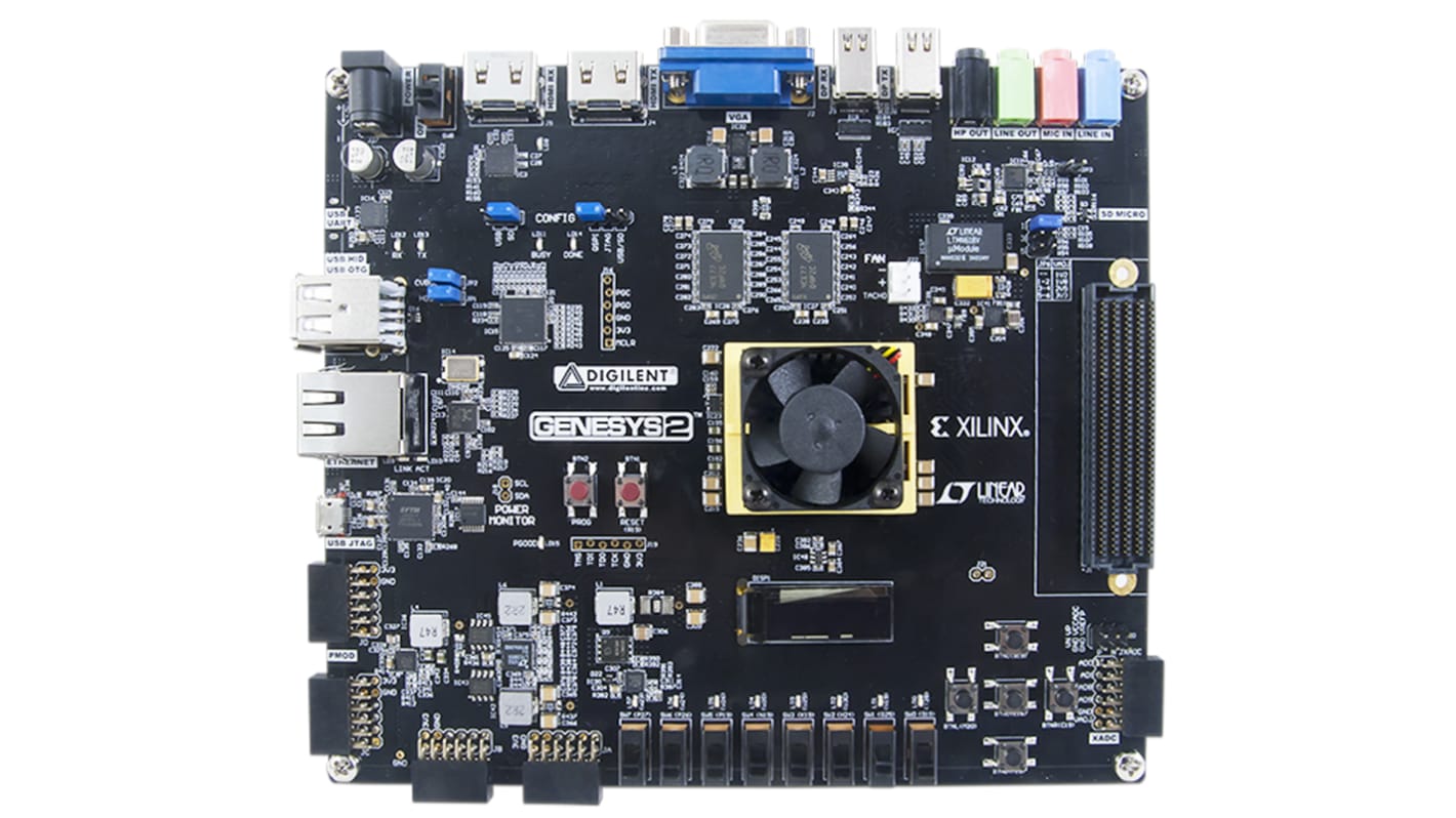
Genesys 2 Kintex-7 FPGA Development Board
The Digilent Genesys 2 board is a digital circuit development platform based on the Kintex-7™ Field Programmable Gate Array (FPGA) from Xilinx. Genesys 2 is well suited for data and video processing applications. Genesys 2 is compatible with Vivado Design Suite as well as the ISE toolset, which includes ChipScope and EDK.
XC7K325T-2FFG900C FPGA Features
• 50950 logic slices each with 4 x 6-input LUTs and 8 x flip-flops
• Close to 16Mbits of fast block RAM
• 10 x clock management tiles, each with phase-locked loop (PLL)
• 840 x DSP slices
• Internal clock speeds exceeding 450MHz
• On-chip analogue-to-digital converter (XADC)
• Up to 10.3125Gbps gigabit transceivers
• 1800Mbps DDR3 data rate with 32-bit data width
• Commercial -2 speed grade
Genesys 2 Board Features
• On-board 2 x MT41J256M16HA-107 1GiB DDR3 SDRAM memory
• On-board S25FL256S 256Mbit Quad-SPI serial NOR Flash memory
• On-board ADAU1761 SigmaDSP stereo audio CODEC
• On-board FT2232R USB-UART bridge controller
• On-board RTL8211E-VL Ethernet PHY
• 0.91in 128 x 32pixel OLED display
• microSD card slot
• On-board USB-JTAG programming via microUSB connector
• JTAG 6-pin header
• RJ45 socket for 10/100/1000 Ethernet LAN
• USB-A OTG 2.0 socket
• USB-A Host MSD/HID socket
• HDMI display (source) socket
• HDMI display (sink) socket
• DisplayPort (source) mDP socket
• DisplayPort (sink) mDP socket
• VGA display (16-bit colour) DE15 socket
• HPC FMC 400-pin connector with 10 x GTX lanes
• 4 x 3.5mm jack sockets for Microphone, Line In, Line Out, Headphones
• 5 x 12-pin Pmod™ expansion connectors
• +12Vdc power supply barrel jack socket
• Cooling fan for FPGA device
• Power slide-switch
• Reset pushbutton
• Programming pushbutton
• 8 x User slide-switches
• 5 x User pushbuttons
• Power LED
• Programming Done LED
• Ethernet Activity LEDs
• 8 x User LEDs
An FPGA is a semiconductor device consisting of a matrix of Configurable Logic Blocks (CLBs) connected through programmable interconnects. The user determines these interconnections by programming SRAM. A CLB can be simple (AND, OR gates, etc) or complex (a block of RAM). The FPGA allows changes to be made to a design even after the device is soldered into a PCB.
Supplied with
USB-A to Micro-B cable
relaterade länkar
- Digilent 410-183 Basys Artix-7 Development Board
- Digilent 410-376 Xilinx Spartan-7 Development Board
- Digilent 410-316 Nexys Video Artix-7 Development Board
- Digilent 410-319-1 FPGA Development Board for Makers and Hobbyists Development Board
- Digilent 410-370 Cora Z7: Zynq-7000 Development Board for ARM Development, FPGA Development
- Digilent 410-292 Nexys A7-100T Nexys 4 DDR Artix-7 Development Board
- Digilent 410-352 Xilinx Spartan-7 Development Board for Hobbyists XC7S25-CSGA324
- Digilent 410-372 Adapter for use with APSoC Development Board, FPGA