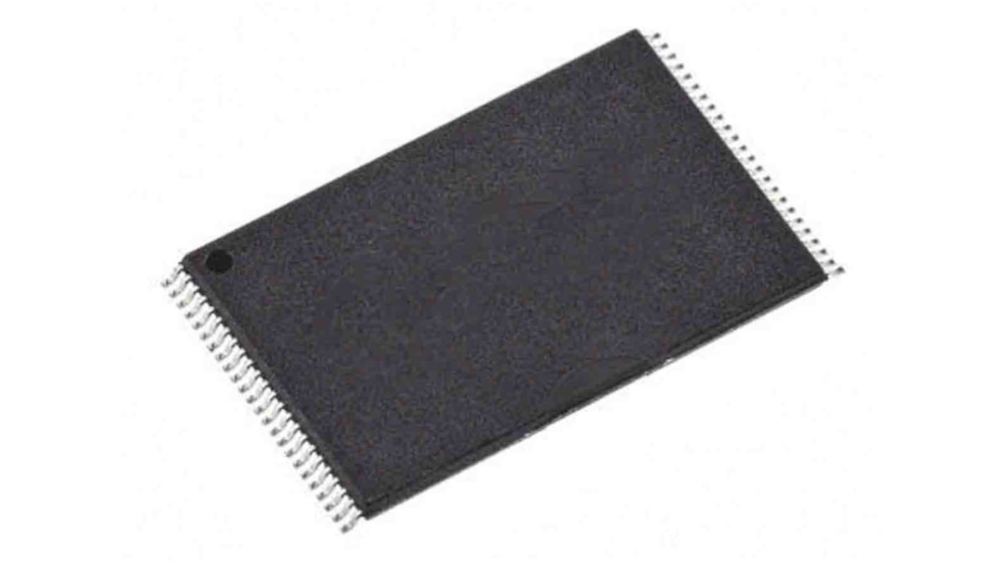
Infineon NOR 8 MB CFI Flash Memory 48-Pin TSOP, S29AL008J70TFI013
- RS-artikelnummer:
- 193-8785
- Tillv. art.nr:
- S29AL008J70TFI013
- Tillverkare / varumärke:
- Infineon

Antal (1 förpackning med 5 enheter)*
127,41 kr
(exkl. moms)
159,26 kr
(inkl. moms)
GRATIS leverans för online beställningar över 500,00 kr
Sista RS lager
- Slutlig(a) 970 enhet(er), redo att levereras
Enheter | Per enhet | Per förpackning* |
|---|---|---|
| 5 + | 25,482 kr | 127,41 kr |
*vägledande pris
- RS-artikelnummer:
- 193-8785
- Tillv. art.nr:
- S29AL008J70TFI013
- Tillverkare / varumärke:
- Infineon
Specifikationer
Datablad
Lagstiftning och ursprungsland
Produktdetaljer
Hitta liknande produkter genom att välja ett eller flera attribut.
Välj alla | Attribut | Värde |
|---|---|---|
| Brand | Infineon | |
| Product Type | Flash Memory | |
| Memory Size | 8MB | |
| Interface Type | CFI | |
| Package Type | TSOP | |
| Pin Count | 48 | |
| Organisation | 1M x 8 Bit | |
| Mount Type | Surface | |
| Cell Type | NOR | |
| Minimum Supply Voltage | 2.7V | |
| Maximum Supply Voltage | 3.6V | |
| Timing Type | Asynchronous | |
| Minimum Operating Temperature | -40°C | |
| Maximum Operating Temperature | 85°C | |
| Standards/Approvals | No | |
| Length | 12mm | |
| Width | 12 mm | |
| Height | 1.05mm | |
| Number of Bits per Word | 8 | |
| Maximum Random Access Time | 70ns | |
| Number of Words | 1M | |
| Automotive Standard | AEC-Q100 | |
| Series | S29AL008J | |
| Supply Current | 20mA | |
| Välj alla | ||
|---|---|---|
Brand Infineon | ||
Product Type Flash Memory | ||
Memory Size 8MB | ||
Interface Type CFI | ||
Package Type TSOP | ||
Pin Count 48 | ||
Organisation 1M x 8 Bit | ||
Mount Type Surface | ||
Cell Type NOR | ||
Minimum Supply Voltage 2.7V | ||
Maximum Supply Voltage 3.6V | ||
Timing Type Asynchronous | ||
Minimum Operating Temperature -40°C | ||
Maximum Operating Temperature 85°C | ||
Standards/Approvals No | ||
Length 12mm | ||
Width 12 mm | ||
Height 1.05mm | ||
Number of Bits per Word 8 | ||
Maximum Random Access Time 70ns | ||
Number of Words 1M | ||
Automotive Standard AEC-Q100 | ||
Series S29AL008J | ||
Supply Current 20mA | ||
- COO (Country of Origin):
- TH
The S29AL008J is a 8 Mbit, 3.0 Volt-only Flash memory organized as 1,048,576 bytes or 524,288 words. The device is offered in 48-ball Fine-pitch BGA (0.8 mm pitch) and 48pin TSOP packages. The word-wide data (x16) appears on DQ15–DQ0, the byte-wide (x8) data appears on DQ7–DQ0. This device is designed to be programmed in-system with the standard system 3.0 volt VCC supply. A 12.0 V VPP or 5.0 VCC are not required for write or erase operations. The device can also be programmed in standard EPROM programmers.
The device offers access times of up to 55 ns allowing high speed microprocessors to operate without wait states. To eliminate bus contention the device has separate chip enable (CE#), write enable (WE#) and output enable (OE#) controls.
Device programming occurs by executing the program command sequence. This initiates the Embedded Program algorithm an internal algorithm that automatically times the program pulse widths and verifies proper cell margin. The Unlock Bypass mode facilitates faster programming times by requiring only two write cycles to program data instead of four.
Device erasure occurs by executing the erase command sequence. This initiates the Embedded Erase algorithm an internal algorithm that automatically preprograms the array (if it is not already programmed) before executing the erase operation. Duringerase, the device automatically times the erase pulse widths and verifies proper cell margin. The host system can detect whether a program or erase operation is complete by observing the RY/BY# pin, or by reading the DQ7(Data# Polling) and DQ6 (toggle) status bits. After a program or erase cycle has been completed, the device is ready to read array data or accept another command.
Relaterade länkar
- Infineon NOR 8Mbit CFI Flash Memory 48-Pin TSOP, S29AL008J70TFI013
- Infineon NOR 8Mbit CFI Flash Memory 48-Pin TSOP, S29AL008J70TFI023
- Infineon NOR 8Mbit CFI S29AL008J70TFI010
- NOR 32Mbit CFI Flash Memory 48-Pin TSOP
- Infineon NOR 32Mbit CFI Flash Memory 48-Pin TSOP, S29JL032J70TFI020
- Infineon NOR 16Mbit CFI Flash Memory 48-Pin TSOP, S29AL016J70TFI023
- Infineon NOR 16Mbit CFI Flash Memory 48-Pin TSOP, S29AL016J70TFI013
- Infineon NOR 8Mbit SPI Flash Memory 48-Pin TSOP, S29AL008J55TFIR20