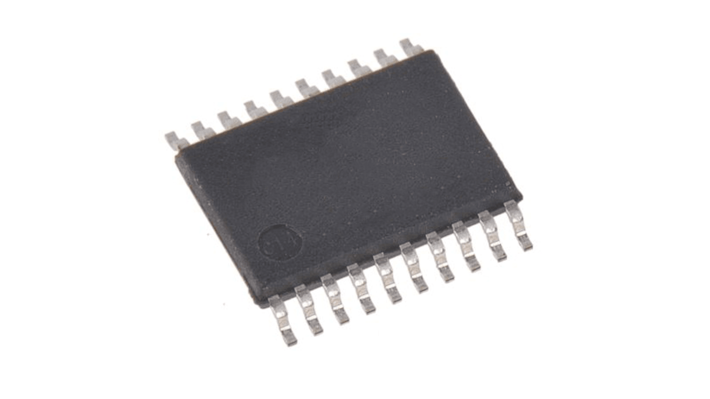
Renesas Electronics 5PB1110PGGI Clock Buffer 20-Pin TSSOP
- RS-artikelnummer:
- 254-4943P
- Tillv. art.nr:
- 5PB1110PGGI
- Tillverkare / varumärke:
- Renesas Electronics

Mängdrabatt möjlig
Antal 10 enheter (levereras i ett rör)*
535,90 kr
(exkl. moms)
669,90 kr
(inkl. moms)
GRATIS leverans för online beställningar över 500,00 kr
Tillfälligt slut
- 10 enhet(er) är redo att levereras
Behöver du mer? Ange den kvantitet du behöver och klicka på "Kontrollera leveransdatum"
Enheter | Per enhet |
|---|---|
| 10 - 18 | 53,59 kr |
| 20 - 24 | 52,47 kr |
| 26 - 72 | 50,625 kr |
| 74 + | 43,735 kr |
*vägledande pris
- RS-artikelnummer:
- 254-4943P
- Tillv. art.nr:
- 5PB1110PGGI
- Tillverkare / varumärke:
- Renesas Electronics
Specifikationer
Datablad
Lagstiftning och ursprungsland
Produktdetaljer
Hitta liknande produkter genom att välja ett eller flera attribut.
Välj alla | Attribut | Värde |
|---|---|---|
| Brand | Renesas Electronics | |
| Maximum Supply Current | 27 mA | |
| Maximum Input Frequency | 200MHz | |
| Mounting Type | Surface Mount | |
| Package Type | TSSOP | |
| Pin Count | 20 | |
| Välj alla | ||
|---|---|---|
Brand Renesas Electronics | ||
Maximum Supply Current 27 mA | ||
Maximum Input Frequency 200MHz | ||
Mounting Type Surface Mount | ||
Package Type TSSOP | ||
Pin Count 20 | ||
The Renesas Electronics high-performance LVCMOS clock buffer has an additive phase jitter of 50 fs RMS. There are five different fan-out variations available that is 1:2 to 1:10. Its supports a synchronous glitch-free output enable (OE) function to eliminate any potential intermediate incorrect output clock cycles when enabling or disabling outputs. It can operate from a 1.8 V to 3.3 V supply.
High-performance 1:2, 1:4, 1:6, 1:8, 1:10 LVCMOS clock buffer
Very low pin-to-pin skew: < 50 ps
Very low additive jitter: < 50 fs
Supply voltage: 1.8 V to 3.3 V
3.3 V tolerant input clock
fMAX is 200 MHz
Integrated serial termination for 50 Ω channel
Packaged in 8-, 14-, 16-, 20-pin TSSOP and as small as 2 x 2 mm DFN and 3 x 3 mm VFQFPN packages
Industrial (-40°C to +85°C) and extended (-40°C to +105°C) temperature ranges
relaterade länkar
- Renesas Electronics 5PB1110PGGI Clock Buffer 20-Pin TSSOP
- Renesas Electronics 9DBL411BGLF Clock Buffer 20-Pin TSSOP
- Renesas Electronics 9DBL411BGILF Clock Buffer 20-Pin TSSOP
- Renesas Electronics 9DB233AGILF Clock Buffer 20-Pin TSSOP
- Renesas Electronics 9DB102BGLF Clock Buffer 20-Pin TSSOP
- Renesas Electronics 9DBL411BGLFT Clock Buffer 20-Pin TSSOP
- Renesas Electronics 9DB102BGLFT PLL Clock Buffer 20-Pin 20-pin TSSOP
- Renesas Electronics 5PB1108PGGK Clock Buffer 16-Pin TSSOP