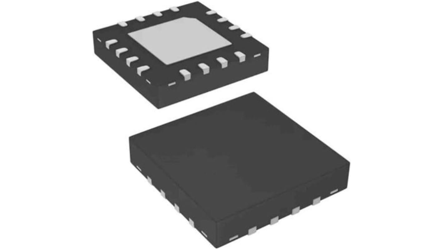
Renesas Electronics 8SLVD1204-33NLGI, LVDS Buffer Quad LVCMOS Buffer, 12-Pin VFQFPN
- RS-artikelnummer:
- 217-7927
- Tillv. art.nr:
- 8SLVD1204-33NLGI
- Tillverkare / varumärke:
- Renesas Electronics

Inte tillgänglig
RS kommer inte längre att lagerföra denna produkt.
- RS-artikelnummer:
- 217-7927
- Tillv. art.nr:
- 8SLVD1204-33NLGI
- Tillverkare / varumärke:
- Renesas Electronics
Specifikationer
Datablad
Lagstiftning och ursprungsland
Produktdetaljer
Hitta liknande produkter genom att välja ett eller flera attribut.
Välj alla | Attribut | Värde |
|---|---|---|
| Brand | Renesas Electronics | |
| Number of Drivers | 4 | |
| Input Type | LVCMOS | |
| Output Type | Buffer | |
| Number of Elements per Chip | 6 | |
| Package Type | VFQFPN | |
| Pin Count | 12 | |
| Välj alla | ||
|---|---|---|
Brand Renesas Electronics | ||
Number of Drivers 4 | ||
Input Type LVCMOS | ||
Output Type Buffer | ||
Number of Elements per Chip 6 | ||
Package Type VFQFPN | ||
Pin Count 12 | ||
The Renesas Electronics IDT8SLVD1204-33I is a high-performance differential LVDS fanout buffer. The device is designed for the fanout of high-frequency, very low additive phase-noise clock and data signals. The IDT8SLVD1204-33I is characterized to operate from a 3.3V power supply. Guaranteed output-to-output and part-to-part skew characteristics make the IDT8SLVD1204-33I ideal for those clock distribution applications demanding well-defined performance and repeatability.
Four low skew, low additive jitter LVDS output pairs
Two selectable differential clock input pairs
Differential PCLKx, nPCLKx pairs can accept the following differential input levels: LVDS, LVPECL
Maximum input clock frequency: 2GHz
LVCMOS/LVTTL interface levels for the control input select pin
Output skew: 20ps (maximum)
Propagation delay: 310ps (maximum)
Low additive phase jitter, RMS
fREF = 156.25MHz, VPP = 1V, 10kHz - 20MHz: 100fs (maximum)