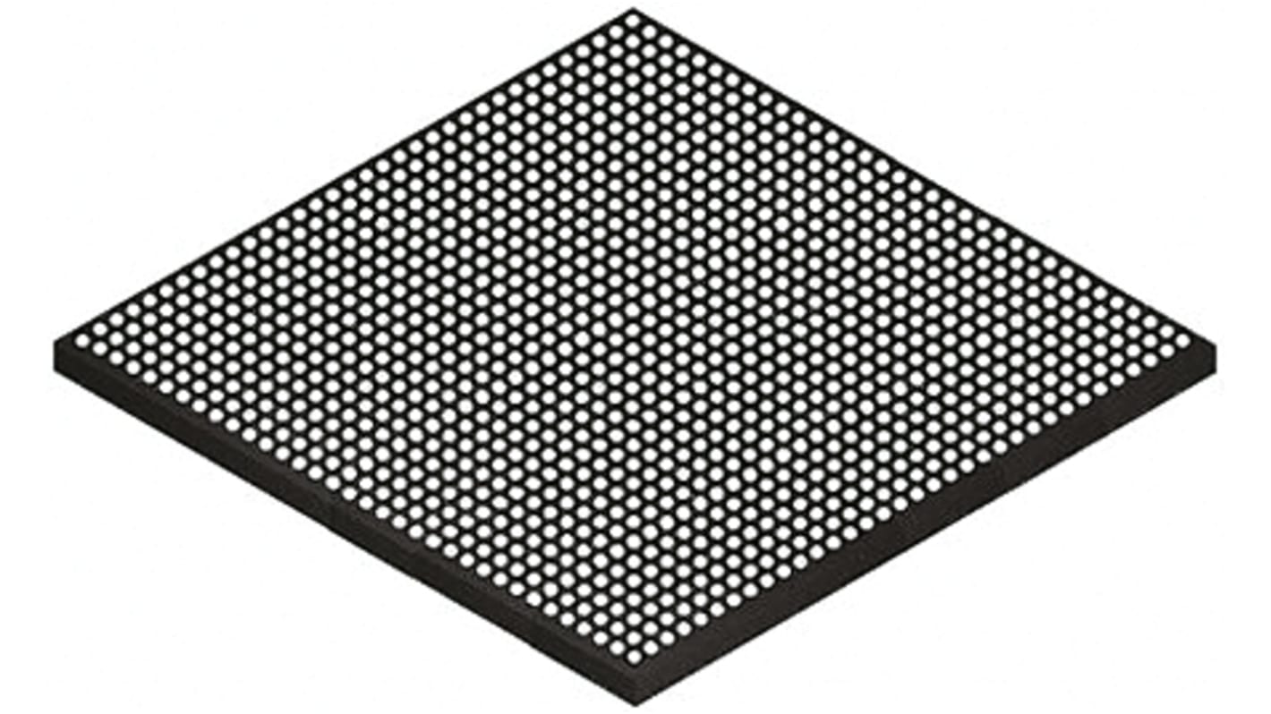
Altera FPGA 5AGXMB1G4F40C4N, Arria V 300000 Cells, 300k Gates, 16952kbit, 300000 Blocks, 1517-Pin FBGA
- RS-artikelnummer:
- 830-3607
- Tillv. art.nr:
- 5AGXMB1G4F40C4N
- Tillverkare / varumärke:
- Altera

Lagerinformation är för närvarande otillgänglig
- RS-artikelnummer:
- 830-3607
- Tillv. art.nr:
- 5AGXMB1G4F40C4N
- Tillverkare / varumärke:
- Altera
Specifikationer
Datablad
Lagstiftning och ursprungsland
Produktdetaljer
Hitta liknande produkter genom att välja ett eller flera attribut.
Välj alla | Attribut | Värde |
|---|---|---|
| Brand | Altera | |
| Family Name | Arria V | |
| Number of Logic Gates | 300k | |
| Number of Logic Cells | 300000 | |
| Number of Logic Units | 300000 | |
| Dedicated DSP | Yes | |
| Number of Registers | 452832 | |
| Number of Multipliers | 1840 (18 x 18), 2760 (9 x 9), 920 (27 x 27) | |
| Mounting Type | Surface Mount | |
| Package Type | FBGA | |
| Pin Count | 1517 | |
| Number of RAM Bits | 16952kbit | |
| Dimensions | 40 x 40 x 2.1mm | |
| Height | 2.1mm | |
| Length | 40mm | |
| Minimum Operating Temperature | 0 °C | |
| Maximum Operating Supply Voltage | 1.13 V | |
| Minimum Operating Supply Voltage | 1.07 V | |
| Maximum Operating Temperature | +85 °C | |
| Width | 40mm | |
| Välj alla | ||
|---|---|---|
Brand Altera | ||
Family Name Arria V | ||
Number of Logic Gates 300k | ||
Number of Logic Cells 300000 | ||
Number of Logic Units 300000 | ||
Dedicated DSP Yes | ||
Number of Registers 452832 | ||
Number of Multipliers 1840 (18 x 18), 2760 (9 x 9), 920 (27 x 27) | ||
Mounting Type Surface Mount | ||
Package Type FBGA | ||
Pin Count 1517 | ||
Number of RAM Bits 16952kbit | ||
Dimensions 40 x 40 x 2.1mm | ||
Height 2.1mm | ||
Length 40mm | ||
Minimum Operating Temperature 0 °C | ||
Maximum Operating Supply Voltage 1.13 V | ||
Minimum Operating Supply Voltage 1.07 V | ||
Maximum Operating Temperature +85 °C | ||
Width 40mm | ||
Arria V GX FPGA with 6Gbps Transceivers, Altera
These devices Provide bandwidth, cost, and power levels that are optimized for high-volume data and signal-processing applications.
An FPGA is a semiconductor device consisting of a matrix of Configurable Logic Blocks (CLBs) connected through programmable interconnects. The user determines these interconnections by programming SRAM. A CLB can be simple (AND, OR gates, etc) or complex (a block of RAM). The FPGA allows changes to be made to a design even after the device is soldered into a PCB.
