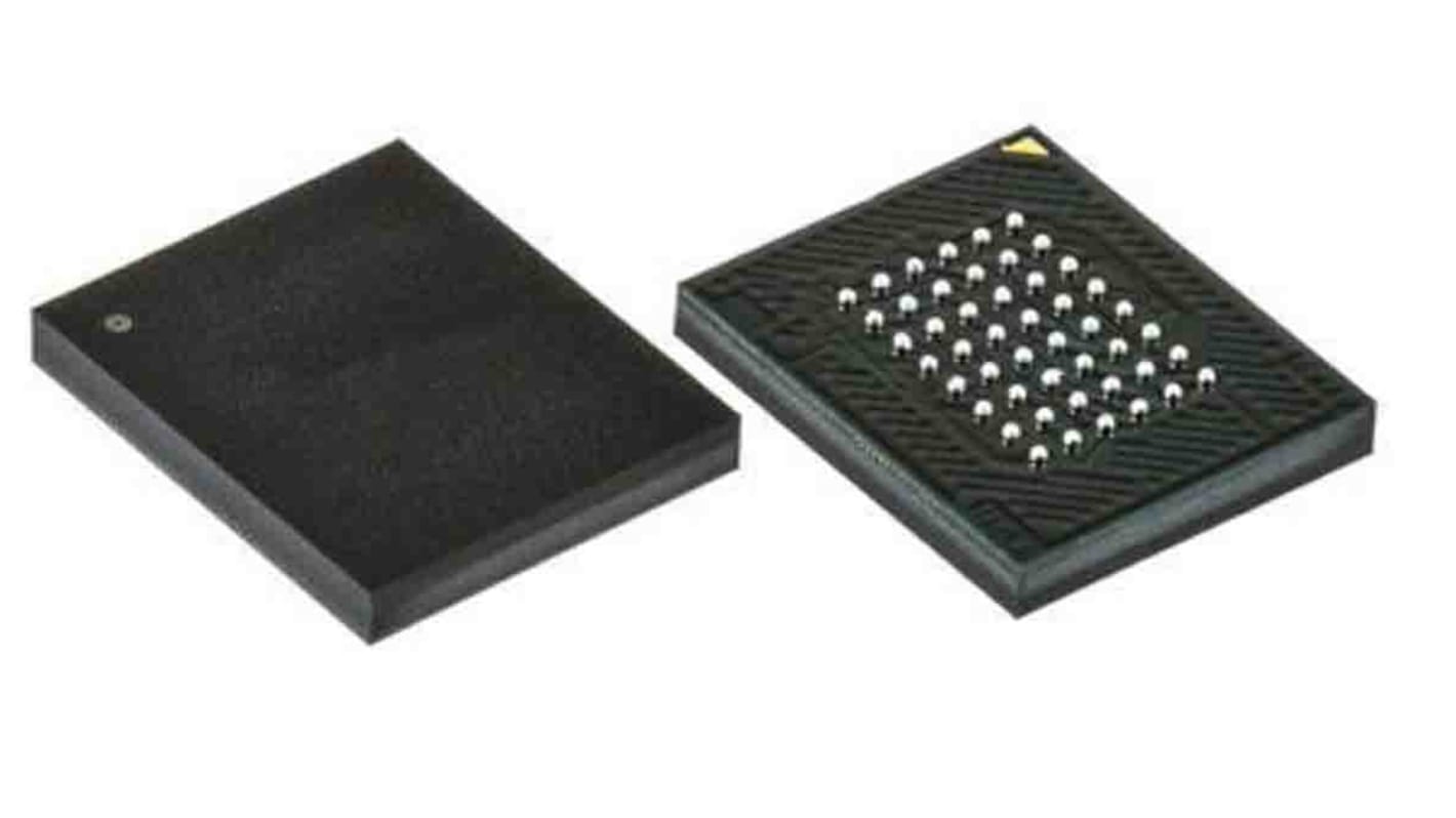
Infineon, CFI, NOR 64 MB Flash-minne, 70 ns, 48 Ben, BGA
- RS-artikelnummer:
- 193-8826
- Tillv. art.nr:
- S29GL064S70BHI030
- Tillverkare / varumärke:
- Infineon

Antal (1 förpackning med 5 enheter)*
196,76 kr
(exkl. moms)
245,95 kr
(inkl. moms)
GRATIS leverans för online beställningar över 500,00 kr
I lager
- 3 285 enhet(er) är redo att levereras
Behöver du mer? Ange den kvantitet du behöver och klicka på "Kontrollera leveransdatum"
Enheter | Per enhet | Per förpackning* |
|---|---|---|
| 5 + | 39,352 kr | 196,76 kr |
*vägledande pris
- RS-artikelnummer:
- 193-8826
- Tillv. art.nr:
- S29GL064S70BHI030
- Tillverkare / varumärke:
- Infineon
Specifikationer
Datablad
Lagstiftning och ursprungsland
Produktdetaljer
Hitta liknande produkter genom att välja ett eller flera attribut.
Välj alla | Attribut | Värde |
|---|---|---|
| Varumärke | Infineon | |
| Produkttyp | Flash-minne | |
| Minnesstorlek | 64MB | |
| Gränssnittstyp | CFI, | |
| Kapseltyp | BGA | |
| Antal ben | 48 | |
| Typ av fäste | Yta | |
| Celltyp | NOR | |
| Maximal matningsspänning | 3.6V | |
| Minsta matningsspänning | 2.7V | |
| Tidsinställningstyp | Asynkron | |
| Minsta arbetsstemperatur | -40°C | |
| Maximal arbetstemperatur | 85°C | |
| Höjd | 0.84mm | |
| Längd | 8.15mm | |
| Standarder/godkännanden | No | |
| Fordonsstandard | AEC-Q100 | |
| Serie | S29GL064S | |
| Matningsström | 50mA | |
| Antal bitar per ord | 8 | |
| Maximal slumpmässig åtkomsttid | 70ns | |
| Antal ord | 8K | |
| Välj alla | ||
|---|---|---|
Varumärke Infineon | ||
Produkttyp Flash-minne | ||
Minnesstorlek 64MB | ||
Gränssnittstyp CFI, | ||
Kapseltyp BGA | ||
Antal ben 48 | ||
Typ av fäste Yta | ||
Celltyp NOR | ||
Maximal matningsspänning 3.6V | ||
Minsta matningsspänning 2.7V | ||
Tidsinställningstyp Asynkron | ||
Minsta arbetsstemperatur -40°C | ||
Maximal arbetstemperatur 85°C | ||
Höjd 0.84mm | ||
Längd 8.15mm | ||
Standarder/godkännanden No | ||
Fordonsstandard AEC-Q100 | ||
Serie S29GL064S | ||
Matningsström 50mA | ||
Antal bitar per ord 8 | ||
Maximal slumpmässig åtkomsttid 70ns | ||
Antal ord 8K | ||
The S29GL-S mid density family of devices are 3.0-volt single-power flash memory manufactured using 65 nm MirrorBit technology.
The S29GL064S is a 64-Mb device organized as 4,194,304 words or 8,388,608 bytes. Depending on the model number, the devices have 16bit wide data bus only, or a 16bit wide data bus that can also function as an 8bit wide data bus by using the BYTE# input.
The devices can be programmed either in the host system or in standard EPROM programmers. Access times as fast as 70 ns are available. Package offerings include 48pin TSOP, 56pin TSOP, 48-ball fine-pitch BGA, and 64-ball Fortified BGA, depending on model number. Each device has separate chip enable (CE#), write enable (WE#) and output enable (OE#) controls. Each device requires only a single 3.0-volt power supply for both read and write functions. In addition to a VCC input, a high-voltage accelerated program (ACC) feature is supported through increased voltage on the WP#/ACC or ACC input. This feature is intended to facilitate system production. Commands are written to the device using standard microprocessor write timing. Write cycles also internally latch addresses and data needed for the programming and erase operations.
The sector erase architecture allows memory sectors to be erased and reprogrammed without affecting the data contents of other sectors. The device is fully erased when shipped from the factory.
The Advanced Sector Protection features several levels of sector protection, which can disable both the program and erase operations in certain sectors.
Relaterade länkar
- Infineon NOR 64 MB Flash-minne 48 Ben, BGA
- Infineon NOR 256 MB Flash-minne 64 Ben, BGA
- Infineon 512 MB Flash-minne 64 Ben, BGA
- Infineon SPI NOR 512 MB Flash-minne 24 Ben 4
- Infineon NOR 8 MB Flash-minne 48 Ben, TSOP
- Infineon NOR 16 MB Flash-minne 48 Ben, TSOP
- Infineon NOR 32 MB Flash-minne 48 Ben, TSOP
- Infineon Parallell NOR 8 MB Flash-minne 48 Ben, TSOP