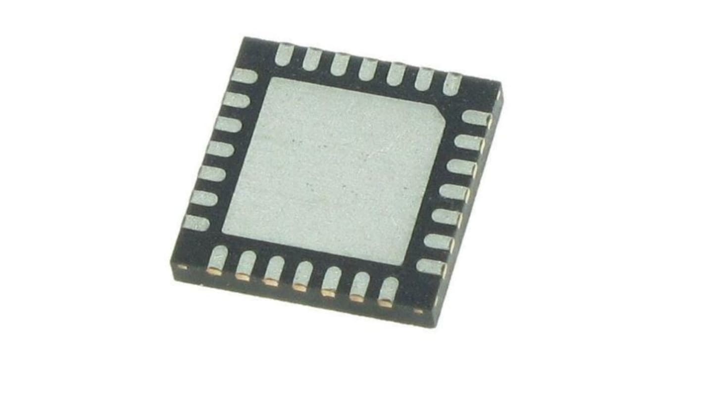
8SLVP1208ANBGI, Clock Buffer LVPECL, 4-Input, 28-Pin LFCSP
- RS-artikelnummer:
- 216-6233
- Tillv. art.nr:
- 8SLVP1208ANBGI
- Tillverkare / varumärke:
- Renesas Electronics

Mängdrabatt möjlig
Antal (1 enhet)*
89,15 kr
(exkl. moms)
111,44 kr
(inkl. moms)
GRATIS leverans för online beställningar över 500,00 kr
I lager
- Dessutom levereras 397 enhet(er) från den 08 januari 2026
Behöver du mer? Ange den kvantitet du behöver och klicka på "Kontrollera leveransdatum"
Enheter | Per enhet |
|---|---|
| 1 - 9 | 89,15 kr |
| 10 - 24 | 80,64 kr |
| 25 - 49 | 71,23 kr |
| 50 - 99 | 69,66 kr |
| 100 + | 66,64 kr |
*vägledande pris
- RS-artikelnummer:
- 216-6233
- Tillv. art.nr:
- 8SLVP1208ANBGI
- Tillverkare / varumärke:
- Renesas Electronics
Specifikationer
Datablad
Lagstiftning och ursprungsland
Produktdetaljer
Hitta liknande produkter genom att välja ett eller flera attribut.
Välj alla | Attribut | Värde |
|---|---|---|
| Brand | Renesas Electronics | |
| Logic Family | LVPECL | |
| Logic Function | Clock Buffer | |
| Input Signal Type | LVPECL | |
| Number of Clock Inputs | 4 | |
| Package Type | LFCSP | |
| Pin Count | 28 | |
| Välj alla | ||
|---|---|---|
Brand Renesas Electronics | ||
Logic Family LVPECL | ||
Logic Function Clock Buffer | ||
Input Signal Type LVPECL | ||
Number of Clock Inputs 4 | ||
Package Type LFCSP | ||
Pin Count 28 | ||
The Renesas Electronics 8SLVP1208 is a high-performance differential LVPECL fanout buffer. The device is designed for the fanout of high-frequency, very low additive phase-noise clock and data signals. The 8SLVP1208 is characterized to operate from a 3.3V and 2.5V power supply. Guaranteed output-to-output and part-to-part skew characteristics make the 8SLVP1208 ideal for those clock distribution applications demanding well-defined performance and repeatability.
Eight low skew, low additive jitter LVPECL output pairs
Two selectable, differential clock input pairs
Differential pairs can accept the following differential input
levels: LVDS, LVPECL, CML
Maximum input clock frequency: 2GHz
LVCMOS interface levels for the control input (input select)
Output skew: 28ps (typical)
Propagation delay: 410ps (maximum)
Low additive phase jitter, RMS: 54.1fs (maximum)
(fREF = 156.25MHz, VPP = 1V, 12kHz - 20MHz)