Infineon CY2308SXI-1 PLL Clock Buffer 16-Pin SOIC
- RS-artikelnummer:
- 194-9013
- Tillv. art.nr:
- CY2308SXI-1
- Tillverkare / varumärke:
- Infineon

För närvarande inte tillgänglig
Vi vet inte om den här artikeln kommer tillbaka i lager, RS har för avsikt att ta bort den från vårt utbud snart.
- RS-artikelnummer:
- 194-9013
- Tillv. art.nr:
- CY2308SXI-1
- Tillverkare / varumärke:
- Infineon
Specifikationer
Datablad
Lagstiftning och ursprungsland
Produktdetaljer
Hitta liknande produkter genom att välja ett eller flera attribut.
Välj alla | Attribut | Värde |
|---|---|---|
| Brand | Infineon | |
| Number of Elements per Chip | 1 | |
| Maximum Supply Current | 45 mA | |
| Maximum Input Frequency | 133.3MHz | |
| Mounting Type | Surface Mount | |
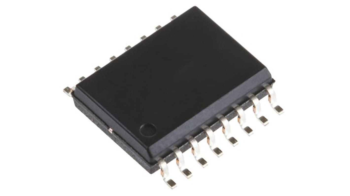
| Package Type | SOIC | |
| Pin Count | 16 | |
| Dimensions | 9.98 x 3.98 x 1.47mm | |
| Length | 9.98mm | |
| Width | 3.98mm | |
| Height | 1.47mm | |
| Maximum Operating Supply Voltage | 3.6 V | |
| Maximum Operating Temperature | +85 °C | |
| Maximum Output Frequency | 100MHz | |
| Minimum Operating Supply Voltage | 3 V | |
| Minimum Output Frequency | 10MHz | |
| Minimum Operating Temperature | -40 °C | |
| Välj alla | ||
|---|---|---|
Brand Infineon | ||
Number of Elements per Chip 1 | ||
Maximum Supply Current 45 mA | ||
Maximum Input Frequency 133.3MHz | ||
Mounting Type Surface Mount | ||
Package Type SOIC | ||
Pin Count 16 | ||
Dimensions 9.98 x 3.98 x 1.47mm | ||
Length 9.98mm | ||
Width 3.98mm | ||
Height 1.47mm | ||
Maximum Operating Supply Voltage 3.6 V | ||
Maximum Operating Temperature +85 °C | ||
Maximum Output Frequency 100MHz | ||
Minimum Operating Supply Voltage 3 V | ||
Minimum Output Frequency 10MHz | ||
Minimum Operating Temperature -40 °C | ||
The CY2308 is a 3.3 V Zero Delay Buffer designed to distribute high speed clocks in PC, workstation, datacom, telecom, and other high performance applications. The part has an on-chip PLL that locks to an input clock presented on the REF pin. The PLL feedback is driven from external FBK pin, so user has flexibility to choose any one of the outputs as feedback input and connect it to FBK pin. The input-to-output skew is less than 250 ps and output-to-output skew is less than 200 ps. The CY2308 has two banks of four outputs each that is controlled by the select inputs as shown in the table Select Input Decoding on page 3. If all output clocks are not required, Bank B is three-stated. The input clock is directly applied to the output for chip and system testing purposes by the select inputs. The CY2308 PLL enters a power down state when there are no rising edges on the REF input. In this mode, all outputs are three-stated and the PLL is turned off resulting in less than 25 μA of current draw.
relaterade länkar
- Infineon CY2308SXI-1H PLL Clock Buffer 16-Pin SOIC
- Infineon CY2308SXI-2 PLL Clock Buffer 16-Pin SOIC
- Infineon CY2308SXI-1 PLL Clock Buffer 16-Pin SOIC
- Infineon CY2292FXI PLL Clock Buffer 16-Pin SOIC
- Infineon CY2292FXC PLL Clock Buffer 16-Pin SOIC
- Infineon CY22392FXC PLL Clock Buffer 16-Pin TSSOP
- Infineon CY2304SXI-1 PLL Clock Buffer 8-Pin SOIC
- Infineon CY23EP05SXI-1H PLL Clock Buffer 8-Pin SOIC