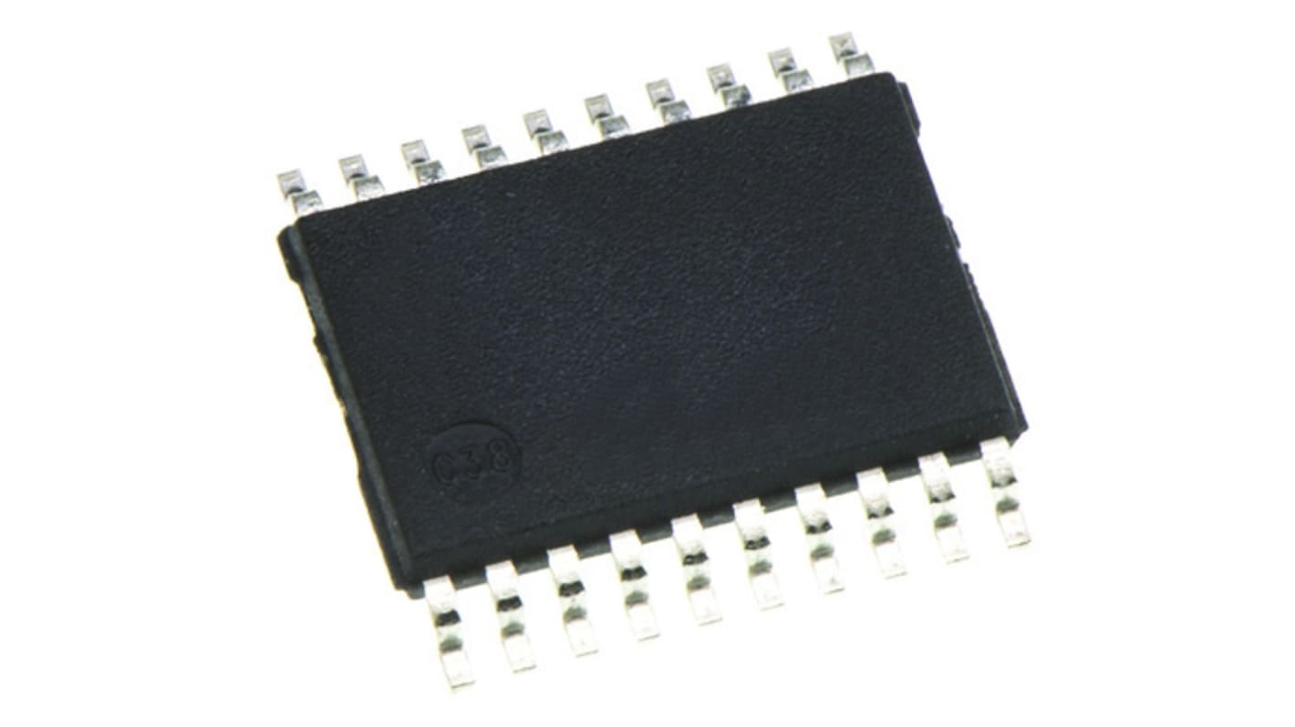
Toshiba 74VHCT245AFT, 18 Bus Transceiver, 8-Bit Non-Inverting CMOS, TTL, 20-Pin TSSOP
- RS-artikelnummer:
- 171-3473P
- Tillv. art.nr:
- 74VHCT245AFT
- Tillverkare / varumärke:
- Toshiba

Antal 25 enheter (levereras på en kontinuerlig remsa)*
86,375 kr
(exkl. moms)
107,975 kr
(inkl. moms)
GRATIS leverans för online beställningar över 500,00 kr
I lager
- Dessutom levereras 4 425 enhet(er) från den 22 december 2025
Behöver du mer? Ange den kvantitet du behöver och klicka på "Kontrollera leveransdatum"
Enheter | Per enhet |
|---|---|
| 25 + | 3,455 kr |
*vägledande pris
- RS-artikelnummer:
- 171-3473P
- Tillv. art.nr:
- 74VHCT245AFT
- Tillverkare / varumärke:
- Toshiba
Specifikationer
Datablad
Lagstiftning och ursprungsland
Produktdetaljer
Hitta liknande produkter genom att välja ett eller flera attribut.
Välj alla | Attribut | Värde |
|---|---|---|
| Brand | Toshiba | |
| Logic Family | 74VHCT | |
| Logic Function | Bus Transceiver | |
| Number of Elements per Chip | 18 | |
| Number of Channels per Chip | 8 | |
| Polarity | Non-Inverting | |
| Mounting Type | Surface Mount | |
| Package Type | TSSOP | |
| Pin Count | 20 | |
| Output Level | CMOS, TTL | |
| Maximum High Level Output Current | -8mA | |
| Maximum Low Level Output Current | 8mA | |
| Maximum Propagation Delay Time @ Maximum CL | 11 ns @ 50 pF | |
| Dimensions | 6.5 x 4.4 x 1mm | |
| Minimum Operating Temperature | -40 °C | |
| Width | 4.4mm | |
| Maximum Operating Temperature | +125 °C | |
| Minimum Operating Supply Voltage | 4.5 V | |
| Automotive Standard | AEC-Q100 | |
| Height | 1mm | |
| Length | 6.5mm | |
| Maximum Operating Supply Voltage | 5.5 V | |
| Propagation Delay Test Condition | 50pF | |
| Välj alla | ||
|---|---|---|
Brand Toshiba | ||
Logic Family 74VHCT | ||
Logic Function Bus Transceiver | ||
Number of Elements per Chip 18 | ||
Number of Channels per Chip 8 | ||
Polarity Non-Inverting | ||
Mounting Type Surface Mount | ||
Package Type TSSOP | ||
Pin Count 20 | ||
Output Level CMOS, TTL | ||
Maximum High Level Output Current -8mA | ||
Maximum Low Level Output Current 8mA | ||
Maximum Propagation Delay Time @ Maximum CL 11 ns @ 50 pF | ||
Dimensions 6.5 x 4.4 x 1mm | ||
Minimum Operating Temperature -40 °C | ||
Width 4.4mm | ||
Maximum Operating Temperature +125 °C | ||
Minimum Operating Supply Voltage 4.5 V | ||
Automotive Standard AEC-Q100 | ||
Height 1mm | ||
Length 6.5mm | ||
Maximum Operating Supply Voltage 5.5 V | ||
Propagation Delay Test Condition 50pF | ||
The 74VHCT245AFT is an advanced high speed CMOS OCTAL BUS TRANSCEIVER fabricated with silicon gate C2MOS technology. It achieves the high speed operation similar to equivalent Bipolar Schottky TTL while maintaining the CMOS low power dissipation. It is intended for two-way asynchronous communication between data busses. The direction of data transmission is determined by the level of the DIR input. The enable input (G) can be used to disable the device so that the busses are effectively isolated. The input voltage are compatible with TTL output voltage. This device may be used as a level converter for interfacing 3.3 V to 5 V system. Input protection and output circuit ensure that 0 V to 5.5 V can be applied to the input and output (Note) (Note) (Note) (Note) pins without regard to the supply voltage. These structure prevents device destruction due to mismatched supply and input/output voltages such as battery back up, etc
Wide operating temperature range: Topr = -40 to 125
High speed: tpd = 4.9 ns (typ.) at VCC = 5.0 V
Low power dissipation: ICC = 2.0 μA (max) at Ta = 25
Compatible with TTL inputs : VIL = 0.8 V (max): VIH = 2.0 V (min)
Power down protection is provided on all inputs and outputs.
Balanced propagation delays: tPLH ≈ tPHL
Low noise: VOLP = 1.0 V (max)
Pin and function compatible with the 74 series (AC/HC/AHC/LV etc.) 245 type